
Ultrathin SrTiO3-based oxide memristor with both drift and diffusive dynamics as versatile synaptic emulators for neuromorphic computing
-
Abstract: Artificial synapses are electronic devices that simulate important functions of biological synapses, and therefore are the basic components of artificial neural morphological networks for brain-like computing. One of the most important objectives for developing artificial synapses is to simulate the characteristics of biological synapses as much as possible, especially their self-adaptive ability to external stimuli. Here, we have successfully developed an artificial synapse with multiple synaptic functions and highly adaptive characteristics based on a simple SrTiO3/Nb: SrTiO3 heterojunction type memristor. Diverse functions of synaptic learning, such as short-term/long-term plasticity (STP/LTP), transition from STP to LTP, learning-forgetting-relearning behaviors, associative learning and dynamic filtering, are all bio-realistically implemented in a single device. The remarkable synaptic performance is attributed to the fascinating inherent dynamics of oxygen vacancy drift and diffusion, which give rise to the coexistence of volatile- and nonvolatile-type resistive switching. This work reports a multi-functional synaptic emulator with advanced computing capability based on a simple heterostructure, showing great application potential for a compact and low-power neuromorphic computing system.
-
Keywords:
- memristor /
- artificial synapse /
- synaptic plasticity /
- associative learning /
- learning-experience
-
1. Introduction
Traditional computing based on the von Neumann architecture faces great challenges in achieving low power consumption, high efficiency, scalability, and highly parallel computing [1]. Inspired by the human brain with high computational efficiency and low energy consumption, great efforts have been paid to develop brain-inspired computing systems to simulate the functions of human brain [2]. The human brain is composed of highly interconnected neurons and synapses, where synapses are the connections between neurons and play a key role in the process of transmitting and processing information [3]. Synaptic plasticity is considered to underlie the learning and memory capability of the human brain [4]. Therefore, preparing artificial synapses that fully simulate the functions of biological synapses is crucial for realizing brain-inspired computing systems.
Memristors are an ideal choice for fabricating artificial synapses because their continuously adjustable conductance naturally resembles biological synaptic plasticity [5]. Recently, many kinds of memristors with different resistive switching mechanisms, including ferroelectric type [6], phase change type [7], metal oxides [5, 8], sulfides [9, 10], etc have been developed to mimic synaptic plasticity characteristics, such as long-term potentiation/depression [7, 11] (LTP/LTD), spike time dependent plasticity [5] and spike rate dependent plasticity [12]. However, most of the reported artificial synapses demonstrate single dynamic features and provide only static or complete volatile resistive switching character, which greatly limits their application in neuromorphic systems. For example, drift memristors, which are generally prepared from oxide dielectric materials, have non-volatile resistance switching and are suitable for application in the readout layer of neural networks where a good retention is necessary [13]. In contrast, the diffusive memristors, which are generally built by embedding metallic clusters within a dielectric matrix [14], exhibit short-term volatility due to the spontaneous relaxation of the metallic ions, and are expected to participate in the dynamic behaviors of neural networks [15], such as reservoir computing, information filtering, and adapting the neural network to the environment. To satisfy diverse functional requirements of brain-inspired neural networks, different types of memristors are usually combined on a monolithic circuit, which will inevitably increase the complexity, the volume, as well as the energy consumption of the circuit. Moreover, different memristors cannot always be combined together due to the incompatibility of the fabrication process. Therefore, preparing versatile memristors with multiple dynamic mechanisms and capable of realizing diverse synaptic functions in a single device is of great significance for achieving advanced functionality in an electronic neuronal network with both high energy efficiency and miniaturization.
In this work, we proposed a memristor based on a simple epitaxial heterostructure SrTiO3/Nb: SrTiO3 with Au/Cr used as the top electrode (abbreviated Au/Cr/STO/NSTO), in which both oxygen vacancy drift and diffusion coexist, giving multiple inherent dynamics. In this memristor-based artificial synapse, diverse synaptic functions, including long-/short-term plasticity (LTP/STP) and the transition from STP to LTP can be realistically simulated and advanced synaptic functions, such as learning-forgetting-relearning behaviors, associative learning and dynamic filtering are further achieved. Our work lays the foundation for realizing compact yet fully functional and low-energy artificial synapses.
2. Methods
Epitaxial STO thin films with a thickness of 4 nm were deposited on (001)-oriented Nb: SrTiO3 (Nb: 0.7 wt%) single-crystalline substrates by pulsed laser deposition using a KrF excimer laser (
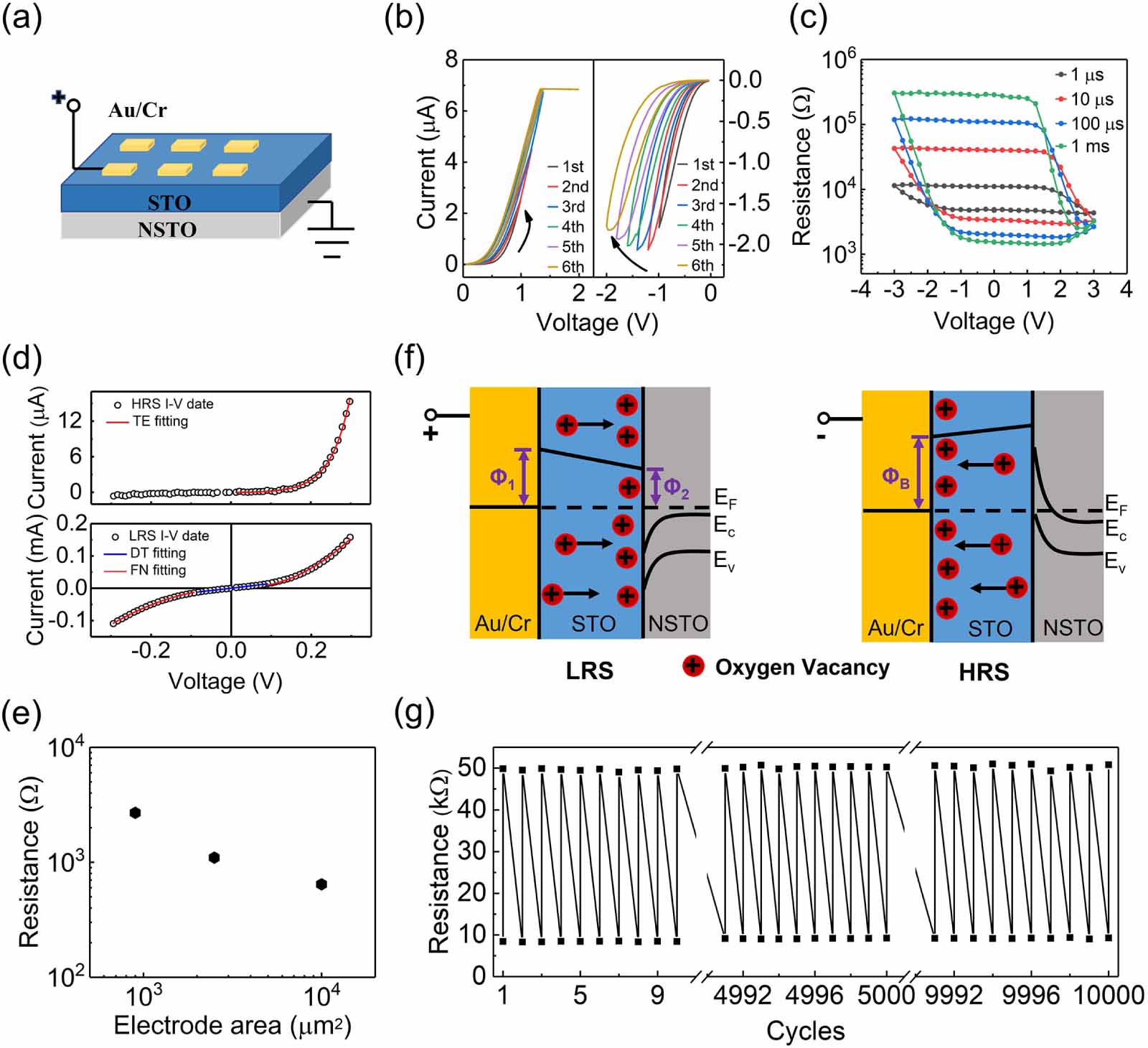
= 248 nm). The STO layer was deposited with a laser energy of 350 mJ with a repetition rate of 2 Hz. Meanwhile, the substrate was kept at a temperature of 780 C under an O2 pressure of 0.04 Torr. Au and Cr top electrodes with thicknesses of 50 and 5 nm and dimensions of 30 30 m2 were deposited on the surface of the STO/NSTO heterostructures by laser direct-writing and vacuum thermal evaporation, and the conductive NSTO substrate services as the bottom electrode. Then, the two-terminal Au/Cr/STO/NSTO memristor is obtained, as illustrated in figure 1(a). ![]() Figure 1. Device structure and the basic electrical characterization. (a) Schematic diagram of Au/Cr/STO/NSTO device. (b) I-V characteristic under positive and negative bias. (c) R-V loops measured with different pulse width. (d) Measured and fitted I-V curves of HRS and LRS for the device. (e) LRS resistance as a function of electrode sizes. (f) Schematic diagram of oxygen vacancy migration and the corresponding energy band diagrams for LRS and HRS. (g) Endurance behavior.
Figure 1. Device structure and the basic electrical characterization. (a) Schematic diagram of Au/Cr/STO/NSTO device. (b) I-V characteristic under positive and negative bias. (c) R-V loops measured with different pulse width. (d) Measured and fitted I-V curves of HRS and LRS for the device. (e) LRS resistance as a function of electrode sizes. (f) Schematic diagram of oxygen vacancy migration and the corresponding energy band diagrams for LRS and HRS. (g) Endurance behavior.The electrical properties of an STO-based memristor were measured using a probe station at ambient conditions by a Keithley 2410 source meter with homemade programs and an ArC ONE system (ArC Instruments). The sample was placed in a probe station with 1
m WG probes. The test pulses were applied to the Au top electrodes, and the NSTO substrates were grounded, where positive voltage means current flow from the Au/Cr metal electrodes to the NSTO substrates. The read voltage was fixed at 0.1 V during all the measurements. 3. Results and discussion
First, the nonlinear transport characteristics of the memristor were evaluated under consecutive positive and negative voltage sweeps. The current-voltage (I-V) curves are shown in figure 1(b), the gradual current increase and decrease under positive and negative voltages confirm the memristive characteristics of the device. To further understand its memristive behavior, the resistance-voltage (R-V) loops were tested. In each loop, the pulse sequence 0
V+max V−max 0 was applied, the lowest resistance state (ON state) is set by +3 V, where the highest resistance state (OFF state) is set by -3 V (figure 1(c)). Multilevel resistance states are achieved by changing the width of the applied pulse sequences. The wide range of intermediate resistance states confirms that our device can achieve multi-level resistance modulation. The I-V curves under low resistance state (LRS) and high resistance state (HRS) are shown in figure 1(d). For the HRS, the thermionic emission (TE) model fits well with the experimental result (figure 1(d), upper panel), thus the TE mode should be the main conduction mechanism, and the height of the Schottky barrier is calculated to be 0.505 eV (supporting information note 1). In contrast, the local I-V curve of the LRS fits well with the direct tunnel (DT) model at the low voltage range (|V| < 0.1 V), and the Fowler-Nordheim tunneling (FNT) model at high voltage range (|V| > 0.1 V) (supporting information note 2). The barrier heights of the DT model at the Cr/STO and STO/NSTO interfaces were 0.36 and 0.47 eV, respectively, and the FNT barrier height was 0.071 eV.For oxides without ferroelectricity, the resistive switching of the STO/NSTO heterostructure should originate from the oxygen vacancy
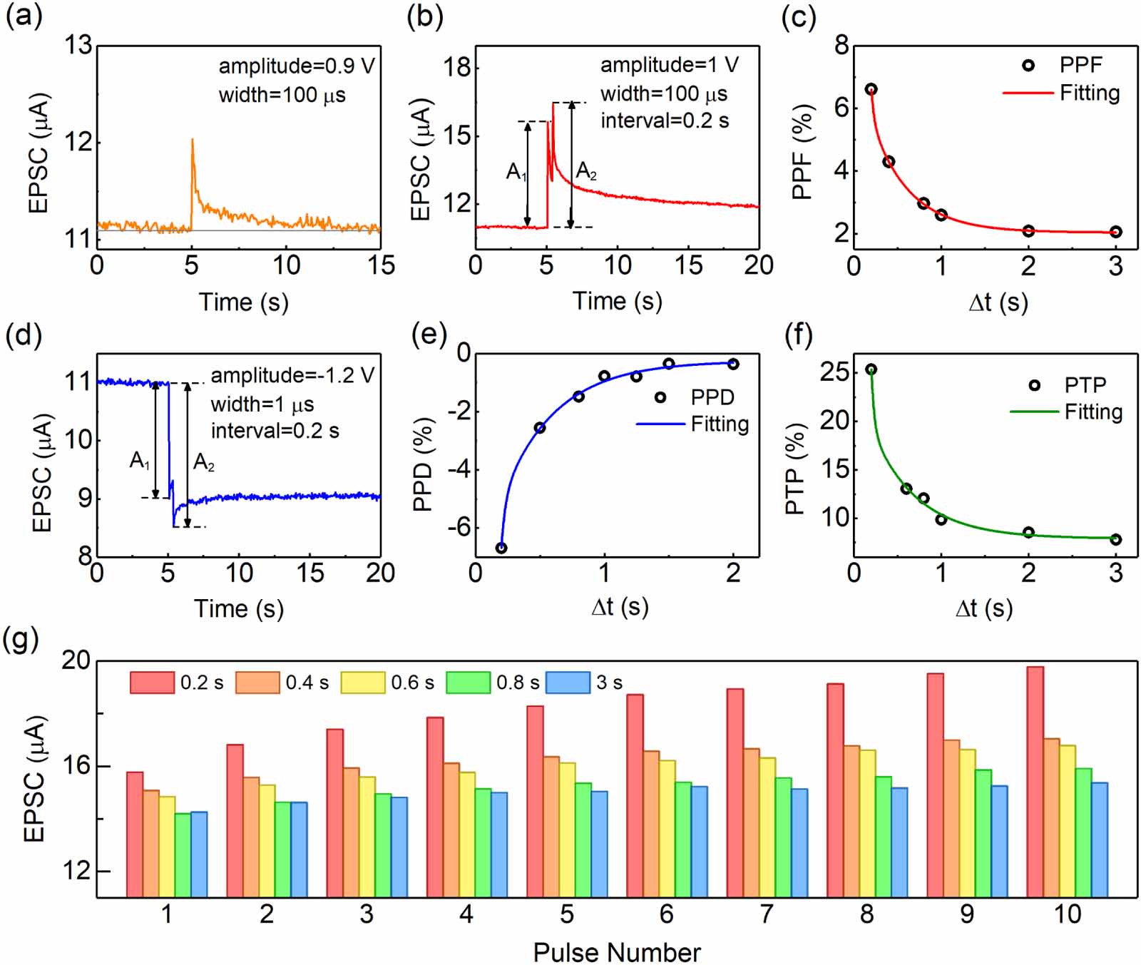
V⋅⋅O migration. Two mechanisms based on theV⋅⋅O migration may be responsible for the resistive switching, the forming/deforming ofV⋅⋅O conductive filaments, and the Schottky barrier variation. In filament-type devices, it should be noted that only one conductive filament channel can be formed under each electrode, so the low-resistance state of the filament-type device is independent of electrode area. In interfacial-type devices, the change in resistance due to the change in the potential barrier at the interface is inversely proportional to the area. To distinguish the two mechanisms, the LRS was tested by varying the top electrode area, results are shown in figure 1(e). It is found that the resistance decreases with increasing electrode area, which confirms the dominant role of the interfacial-type conduction mechanism and excludes the filamentary conduction mechanism [16]. The energy band diagrams of LRS and HRS for Au/Cr/STO/NSTO are shown in figure 1(f). When the positive pulse is applied to the top electrode, the positively chargedV⋅⋅O s migrate to the STO/NSTO interface, an electron accumulation layer is formed at the NSTO side, and the energy barrier at the STO/NSTO interface is reduced. Thus, the average tunneling barrier is decreased, forming the LRS. When a negative voltage is applied, theV⋅⋅O s moves toward the top electrode and accumulates at the Cr/STO interface, resulting in an enhanced energy barrier at the STO/NSTO interface and forming the electron depletion layer in the NSTO. Thus, both tunneling barrier height and width are increased, causing the HRS. In addition, endurance is an important indicator to assess the reliability of the device. Figure 1(g) shows the endurance of the device by alternatively applying +1.8 V and -1.8 V with a pulse width of 100s. The schematic diagram of the test pulse is shown in figure S1. The results demonstrate the excellent durability of the Au/Cr/STO/NSTO memristor without resistance decline up to 104 cycles. Depending on the retention time, synaptic plasticity can be divided into two types: STP and LTP. STP acts on a timescale of tens of milliseconds to a few minutes, it allows the synapse to perform some critical functions, such as fast response and information filtering [ 17 ]. Figure2 (a) shows the excitatory postsynaptic current (EPSC) obtained by applying a single pulse of 0.9 V, 100s. It shows an abrupt increase, followed by a decay to the initial state within 10 s, which is a typical STP phenomenon. The memristor undergoes the following dynamic process to form STP: under the stimulus of a small positive pulse, a handful of V⋅⋅O s drift toward the NSTO side to form a concentration gradient in the STO layer, which would decrease the average energy barrier, giving rise to the abruptly enhanced EPSC. After the pulse is removed,V⋅⋅O s diffuse gradually back to the initial state under the driven concentration gradient; correspondingly, the EPSC decays to the initial value. There are also three other important forms of STP, paired-pulse facilitation (PPF), paired-pulse depression (PPD) and post-tetanic potentiation (PTP). PPF and PPD describe the synaptic weight enhancement and suppression caused by the second pulse relative to that caused by the first one, respectively. Simulations of PPF and PPD are shown in figures2 (b)-(e). PPF and PPD are defined by the equation [18 ]: PPF/PPD = (A 2 -A 1)/A 1 100%, whereA 1 andA 2 are the peak EPSCs of the first and the second spikes, respectively. Both the PPF and PPD index exhibit exponential changes with pulse intervalt [19 ] (figures2 (c) and (e)): PPF/PPD=1+C1e−Δtτ1+C2e−Δtτ2
(1) ![]() Figure 2. Short-term plasticity of the Au/Cr/STO/NSTO artificial synapse. (a) EPSC triggered by a single pulse of 0.9 V, 100
Figure 2. Short-term plasticity of the Au/Cr/STO/NSTO artificial synapse. (a) EPSC triggered by a single pulse of 0.9 V, 100s. (b) The EPSCs triggered by a pair of positive pulses of 1 V, 100 s. (c) The varying of PPF as a function of the relative pulse interval t. (d) The EPSCs triggered by a pair of negative pulses of -1.2 V, 1 ms. (e) The variation of PPD as a function of t. (f) PTP as a function of t, and (g) EPSC under ten pulse stimulations with different pulse frequencies. where C1 and C2 are the initial facilitation magnitudes, and
1 and 2 are the characteristic relaxation times. By fitting PPF, 1 = 32 ms, 2 = 439 ms were obtained. For PPDs, we achieve 1 = 31 ms 2 = 416 ms. The relaxation time of our devices is comparable to that of biological synapses, where relaxation can be divided into a rapid phase lasting tens of milliseconds and a slower phase lasting hundreds of milliseconds [20]. PTP describes the enhancement of the synaptic weight caused by the tenth pulse relative to that caused by the first one. PTP happens when a relatively long high-frequency stimuli train is applied to the presynaptic neuron, where the enhancement of EPSC persists for tens of minutes [17]. The EPSC versus stimulation number is shown in figure 2(g). The tenth pulse caused significantly higher EPSC than the first pulse, which is similar to the biological synapse. The PTP can be calculated by the formula PTP = (A10 - A1)/A1 100%, where A1 and A10 are the peak EPSCs of the first and the tenth spikes, respectively. Moreover, the peak value of EPSC increases with the decrease of the pulse interval t of the stimulus sequence. As t increases, the enhancement capacity of the synaptic weight gradually weakens, being consistent with the biological synapses [21]. The relationship between the PTP and the pulse interval t can also be fitted by equation (1), and the results are shown in figure 2(f). Fitting of PTP gives
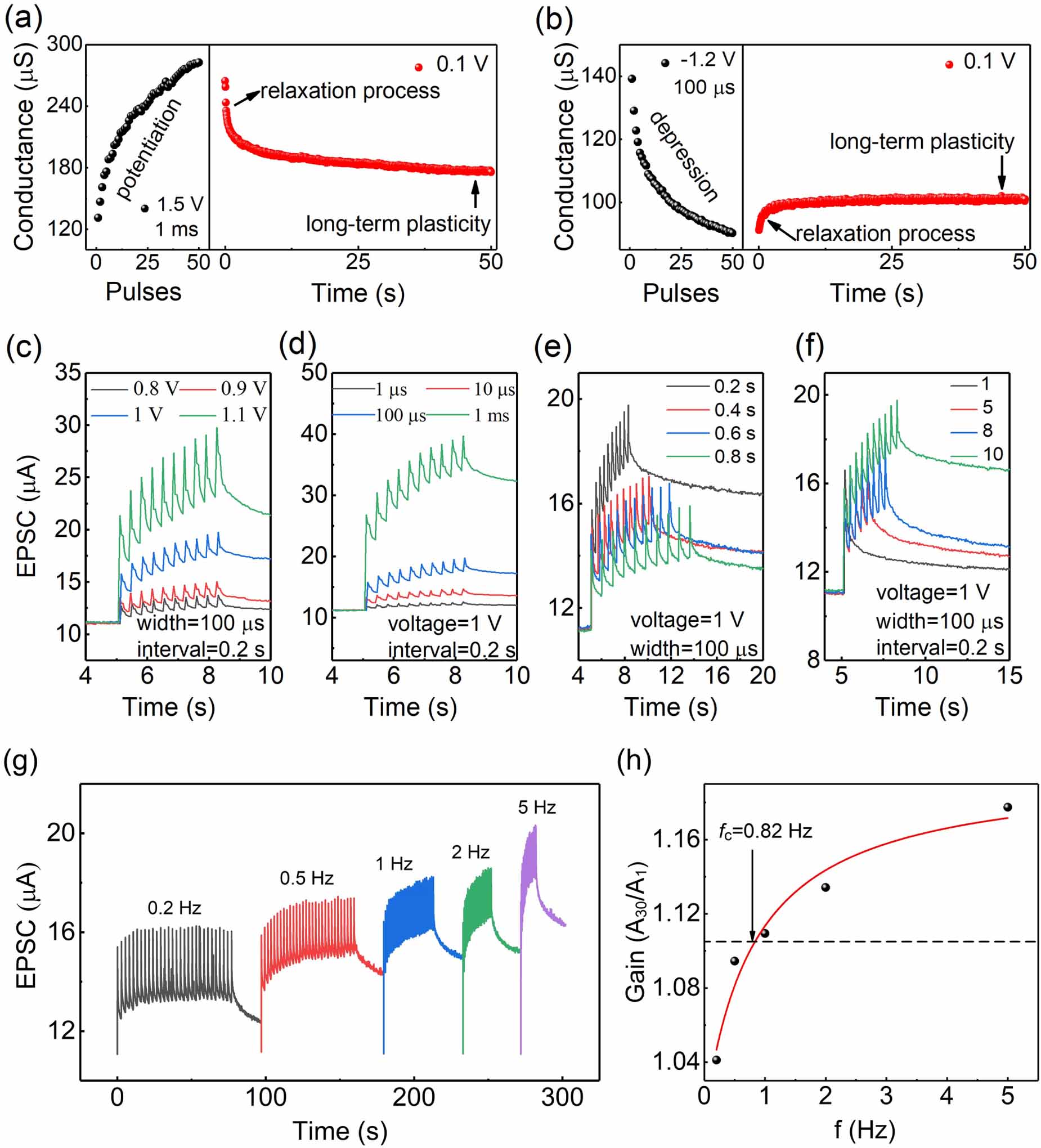
1 = 32 ms, 2 = 526 ms. LTP lasts from hours to a lifetime and is considered to be the foundation of learning and memory in the human brain. By increasing the amplitude, width, frequency, or number of the pulse stimuli, the persistence of synaptic weights is greatly prolonged, and LTP can be achieved. Figures 3(a) and (b) demonstrate two typical kinds of LTP, LTP and LTD, respectively. For the LTP, 50 positive pulses of 1.5 V, 1 ms are applied to the device to form a weight potentiation, and after the spontaneous relaxation process, the weight is retained at 176
s, higher than the initial state, forming a transition from STP to LTP. In contrast, 50 negative pulses of -1.2 V, 100 s induce synaptic depression in the device, after the relaxation process, the final conductance is lower than the initial one, giving LTD (figure 3(b)). Figures 3(c)-(f) show the dependence of the EPSC response on the pulse amplitude, width, time interval, and number of pulses after repeated stimulation. The EPSC increases rapidly after each stimulation and decays gradually with time. With the increase in the pulse amplitude, width and number or the decrease in the pulse interval, larger EPSCs and higher final states are obtained. All final states are higher than the initial state, showing LTP characteristics. ![]() Figure 3. Long-term plasticity of the Au/Cr/STO/NSTO artificial synapse. (a) and (b) Long-term potentiation and long-term depression, respectively. EPSC response to the pulse sequence with different (c) pulse amplitude, (d) pulse width, (e) pulse interval, and (f) pulse number. (g) The EPSC triggered by 30 consecutive pulses with different frequencies. (h) Frequency dependence of EPSC gain A30/A1 and the fitting results by the sigmoidal-shaped function.
Figure 3. Long-term plasticity of the Au/Cr/STO/NSTO artificial synapse. (a) and (b) Long-term potentiation and long-term depression, respectively. EPSC response to the pulse sequence with different (c) pulse amplitude, (d) pulse width, (e) pulse interval, and (f) pulse number. (g) The EPSC triggered by 30 consecutive pulses with different frequencies. (h) Frequency dependence of EPSC gain A30/A1 and the fitting results by the sigmoidal-shaped function.In biological synapses, the release of neurotransmitters during information transmission is mainly determined by the frequency of the stimulus signal. Synaptic vesicles with low release probability can respond to high-frequency signals and release neurotransmitters, giving rise to the high pass filtering function of biological synapses [22]. Figure 3(g) shows the EPSC caused by 30 consecutive pulses with frequency variation from 0.2 to 5 Hz. The increase of the EPSC during the stimulation at a specific frequency is evaluated by using gain A30/A1, which is the ratio of the peak EPSC evoked by the 30th spike (A30) to that evoked by the first one (A1). Figure 3(h) shows that the gain A30/A1 at various frequencies. The frequency dependence of EPSC gain g(f) can be well fitted by a sigmoidal-shaped function g(f) = (a1 - a2)/(1 + (f/fc)p) + a2 [23], where p= 1 is the order of the function, fc is the cut-off frequency, a1 and a2 are respectively the initial and final peak EPSC amplitude. The cut-off frequency fc is determined to be 0.82 Hz. This indicates the dynamic filtering capability of our artificial synapse, that is to say when input signals with a frequency lower than fc, the signal is weakened at the output, while the frequency is higher than fc, the signal is strengthened. Therefore, our device can be used as a high-pass filter for signal processing.
The learning-forgetting-relearning process is an important adaptive function of the brain. It describes the phenomenon that relearning is easier than the initial learning, and how each subsequent relearning can reduce the forgetting rate and strengthen the memory. When performing relearning sessions, the subsequent forgetting rate depends on the repetition order [18] (learning history). The higher the degree of primitive learning, the slower the forgetting rate. In our work, the learning-forgetting-relearning process was simulated by stimulating the memristor with voltage pulses. We define the conductance increase process with stimulus pulse as learning’; the current decay process after removing the electrical pulses is defined as forgetting’. As shown in figure 4, after being stimulated by 50 consecutive voltage pulses, the first learning stage is finished with conductance increases from 485
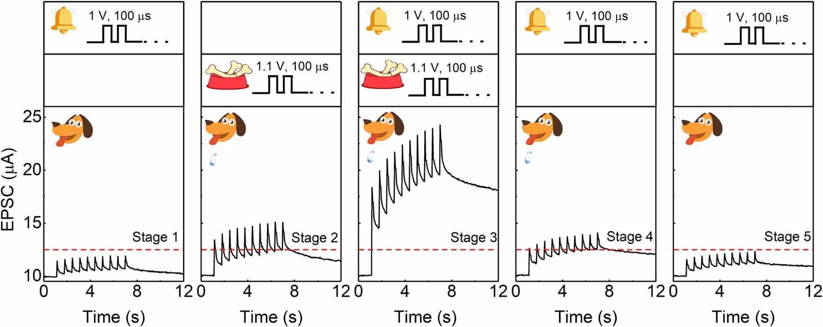
s to 645 s (figure 4(a)). Then, a forgetting process happens, where the conductance decayed spontaneously to 541 s within 10 s (figure 4(b)). In the second learning state, it takes only 17 stimulations to recover to the level of the first learning stage (figure 4(c)), indicating that the relearning process becomes much easier [24]. During the following second forgetting process, the conductance reduced to 560 s within 10 s, and remains at a higher value than the former one (figure 4(d)). In the third learning stage, eight stimuli were enough to restore the previous memory level (figure 4(e)). The third forgetting stage (figure 4(f)) shows the slowest conductivity relaxation and stays at 583 s after 10 s. The results show that our memristor vividly mimics the learning-forgetting-relearning processes of a biological system. It is noteworthy that the learning-forgetting-relearning process is performed by complex neural networks in the brain, but is reproduced in our work by only one nano-electronic device, verifying the powerful function of the Au/Cr/STO/NSTO memristor due to its multi-inherent dynamics. Figure 4. The learning-forgetting-relearning process achieved within a single Au/Cr/STO/NSTO memristor. (a), (c) and (e) Demonstrate the first, second and third learning stage, while (b), (d) and (f) give the first, second and third forgetting process. The amplitude and duration of the voltage pulses are 0.8 V and 100s, respectively. The conductance responses are monitored with a small voltage of 0.1 V. Associative learning is another important function that is responsible for cognition and adaptability of the brain that prepares biological bodies for possible or anticipated events [25]. The famous Pavlov’ dog experiment is a classic form of associative learning. The experiment established the association between implicit memory (a kind of long-term memory) and unconscious memory achieved by training neural networks. In Pavlovian experiments, the bone and the bell were called unconditional stimulus (US) and neutral stimuli (NS), respectively. Before training, the dogs salivated in response to unconditioned stimuli, but not to NS. During training, the dogs were trained to salivate with the continuous triggering of NS before US, which established the association between NS and US. Finally, NS can also trigger salivation in dogs alone like unconditioned stimuli, called acquisition. This Pavlov’ dog experiment is implemented in our device, results are shown in figure 5. First, the EPSC value of 12.5
A was defined as the threshold current of the dog’s salivation response (the red dotted line in figure 5). Here, the bone is simulated by a pulse of 1.1 V, 100 s, while the bell is simulated by a pulse of 1 V, 100 s. When the bell rung’ alone, the current stays below the threshold value (stage 1), suggesting that the bell failed to activate salivation. On the contrary, when feeding the dog alone, the current rises above the threshold value (stage 2), thus triggers salivation’. In order to establish associative learning, the dog was trained by simultaneously feeding’ and ringing the bell’ (stage 3). After training, salivation can be induced by the bell stimuli alone (stage 4), forming the acquisition’. Later, the value of the EPSC with only the ringing stimulus is reduced to below the threshold value, mimicking the disassociation process due to the forgetting behavior of biological brain (stage 5). Based on the above experimental results, Pavlov’s classical conditioning is successfully simulated. ![]() Figure 5. Schematic diagram of Pavlov’s dog experiment, where the bone’ and bell’ stimuli are simulated by the pulses of 1.1 V, 100
Figure 5. Schematic diagram of Pavlov’s dog experiment, where the bone’ and bell’ stimuli are simulated by the pulses of 1.1 V, 100s and 1 V, 100 s, respectively. The displayed current values were obtained under the reading voltage of 0.1 V. 4. Conclusion
In summary, we proposed an Au/Cr/STO/NSTO memristor, which incorporates multiple internal dynamics, including the drift and back-diffusion, enabling the device with diverse synaptic plasticity functions and highly adaptive properties. Our device can not only bio-realistically simulate basic synaptic functions, such as STP, LTP, and dynamic filtering, but also realize the adaptive learning and memory functions of biological neural network in a single device, such as the learning-forgetting-relearning process and associative learning. These results suggest that our artificial synapses with diverse synaptic functions but simple structure are potential candidates for versatile neuromorphic computing devices.
5. Future perspectives
Brain-inspired neuromorphic systems provide a promising approach for confronting the speed and energy consumption bottlenecks of von Neumann architectures. Many neuromorphic systems demand electronic devices with multiple dynamics to achieve the desired functions. However, diverse requirements, such as the co-existence of volatile and non-volatile switching dynamics can hardly be achieved in individual memristive devices. Hence, the realization of targeted applications usually relies on tailored neural circuit designs composed of memristors with various dynamic properties, limiting the development of compact and low-power neuromorphic systems. It is of great importance to integrate multiple inherent dynamics in an individual device and develop multi-functional neuromorphic devices, such as a versatile synaptic emulator that can fully simulate the functions of biological synapses at single device level. The universality of the device can increase the computational complexity of the system without escalating the material and area budget and achieve highly efficient computing in biological nervous systems. The development of devices with more complex dynamic properties is a crucial approach toward realizing a brain-like computing system.
Acknowledgments: The authors acknowledge the support from the National Key Research & Development Program of China (No. 2021YFB3601504), the National Natural Science Foundation of China (Nos. 52072218, 12222414, 12074416), the Natural Science Foundation of Shandong province (Nos. ZR2022YQ43 and ZR2020ZD28), Heilongjiang Provincial Natural Resources Foundation Joint Guide Project (No. LH2020E098), and Peixin Fund of Qilu University of Technology (Shandong Academy of Sciences) (No. 2023PY093). -
![]()
Figure 1. Device structure and the basic electrical characterization. (a) Schematic diagram of Au/Cr/STO/NSTO device. (b) I-V characteristic under positive and negative bias. (c) R-V loops measured with different pulse width. (d) Measured and fitted I-V curves of HRS and LRS for the device. (e) LRS resistance as a function of electrode sizes. (f) Schematic diagram of oxygen vacancy migration and the corresponding energy band diagrams for LRS and HRS. (g) Endurance behavior.
![]()
Figure 2. Short-term plasticity of the Au/Cr/STO/NSTO artificial synapse. (a) EPSC triggered by a single pulse of 0.9 V, 100
s. (b) The EPSCs triggered by a pair of positive pulses of 1 V, 100 s. (c) The varying of PPF as a function of the relative pulse interval t. (d) The EPSCs triggered by a pair of negative pulses of -1.2 V, 1 ms. (e) The variation of PPD as a function of t. (f) PTP as a function of t, and (g) EPSC under ten pulse stimulations with different pulse frequencies. ![]()
Figure 3. Long-term plasticity of the Au/Cr/STO/NSTO artificial synapse. (a) and (b) Long-term potentiation and long-term depression, respectively. EPSC response to the pulse sequence with different (c) pulse amplitude, (d) pulse width, (e) pulse interval, and (f) pulse number. (g) The EPSC triggered by 30 consecutive pulses with different frequencies. (h) Frequency dependence of EPSC gain A30/A1 and the fitting results by the sigmoidal-shaped function.
Figure 4. The learning-forgetting-relearning process achieved within a single Au/Cr/STO/NSTO memristor. (a), (c) and (e) Demonstrate the first, second and third learning stage, while (b), (d) and (f) give the first, second and third forgetting process. The amplitude and duration of the voltage pulses are 0.8 V and 100
s, respectively. The conductance responses are monitored with a small voltage of 0.1 V. -
[1] Wang J R, Zhuge F 2019 Memristive synapses for brain-inspired computing Adv. Mater. Technol. 4 1800544 DOI: 10.1002/admt.201800544
[2] Xi F B, Han Y, Liu M S, Bae J H, Tiedemann A, Grützmacher D, Zhao Q T 2021 Artificial synapses based on ferroelectric Schottky barrier field-effect transistors for neuromorphic applications ACS Appl. Mater. Interfaces 13 32005-12 DOI: 10.1021/acsami.1c07505
[3] Zhang H Z, Ju X, Yew K S, Ang D S 2020 Implementation of simple but powerful trilayer oxide-based artificial synapses with a tailored bio-synapse-like structure ACS Appl. Mater. Interfaces 12 1036-45 DOI: 10.1021/acsami.9b17026
[4] Pereda A E 2014 Electrical synapses and their functional interactions with chemical synapses Nat. Rev. Neurosci. 15 250-63 DOI: 10.1038/nrn3708
[5] Chang T, Jo S H, Lu W 2011 Short-term memory to long-term memory transition in a nanoscale memristor ACS Nano 5 7669-76 DOI: 10.1021/nn202983n
[6] Yang S T, et al 2022 High-performance neuromorphic computing based on ferroelectric synapses with excellent conductance linearity and symmetry Adv. Funct. Mater. 32 2202366 DOI: 10.1002/adfm.202202366
[7] Kuzum D, Jeyasingh R G D, Lee B, Wong H S P 2012 Nanoelectronic programmable synapses based on phase change materials for brain-inspired computing Nano Lett. 12 2179-86 DOI: 10.1021/nl201040y
[8] Sokolov A S, Jeon Y R, Kim S, Ku B, Choi C 2019 Bio-realistic synaptic characteristics in the cone-shaped ZnO memristive device NPG Asia Mater. 11 1-15 DOI: 10.1038/s41427-018-0105-7
[9] Ohno T, Hasegawa T, Tsuruoka T, Terabe K, Gimzewski J K, Aono M 2011 Short-term plasticity and long-term potentiation mimicked in single inorganic synapses Nat. Mater. 10 591-5 DOI: 10.1038/nmat3054
[10] Nayak A, Ohno T, Tsuruoka T, Terabe K, Hasegawa T, Gimzewski J K, Aono M 2012 Controlling the synaptic plasticity of a Cu2S gap-type atomic switch Adv. Funct. Mater. 22 3606-13 DOI: 10.1002/adfm.201200640
[11] Li J K, Ge C, Du J Y, Wang C, Yang G Z, Jin K J 2020 Reproducible ultrathin ferroelectric domain switching for high-performance neuromorphic computing Adv. Mater. 32 1905764 DOI: 10.1002/adma.201905764
[12] Yang Y, Wen J, Guo L Q, Wan X, Du P F, Feng P, Shi Y, Wan Q 2016 Long-term synaptic plasticity emulated in modified graphene oxide electrolyte gated IZO-based thin-film transistors ACS Appl. Mater. Interfaces 8 30281-6 DOI: 10.1021/acsami.6b08515
[13] John R A, et al 2022 Reconfigurable halide perovskite nanocrystal memristors for neuromorphic computing Nat. Commun. 13 2074 DOI: 10.1038/s41467-022-29727-1
[14] Wang Z R, et al 2017 Memristors with diffusive dynamics as synaptic emulators for neuromorphic computing Nat. Mater. 16 101-8 DOI: 10.1038/nmat4756
[15] Midya R, et al 2019 Artificial neural network (ANN) to spiking neural network (SNN) converters based on diffusive memristors Adv. Electron. Mater. 5 1900060 DOI: 10.1002/aelm.201900060
[16] Li J K, Li N, Ge C, Huang H Y, Sun Y W, Gao P, He M, Wang C, Yang G Z, Jin K J 2019 Giant electroresistance in ferroionic tunnel junctions iScience 16 368-77 DOI: 10.1016/j.isci.2019.05.043
[17] Yang R, Huang H M, Guo X 2019 Memristive synapses and neurons for bioinspired computing Adv. Electron. Mater. 5 1900287 DOI: 10.1002/aelm.201900287
[18] Liu G, Wang C, Zhang W B, Pan L, Zhang C C, Yang X, Fan F, Chen Y, Li R W 2016 Organic biomimicking memristor for information storage and processing applications Adv. Electron. Mater. 2 1500298 DOI: 10.1002/aelm.201500298
[19] Yang J T, Ge C, Du J Y, Huang H Y, He M, Wang C, Lu H B, Yang G Z, Jin K J 2018 Artificial synapses emulated by an electrolyte-gated tungsten-oxide transistor Adv. Mater. 30 1801548 DOI: 10.1002/adma.201801548
[20] Liu Y H, Zhu L Q, Feng P, Shi Y, Wan Q 2015 Freestanding artificial synapses based on laterally proton-coupled transistors on chitosan membranes Adv. Mater. 27 5599-604 DOI: 10.1002/adma.201502719
[21] Shen Z H, Li W H, Tang X G, Hu J, Wang K Y, Jiang Y P, Guo X B 2022 An artificial synapse based on Sr(Ti, Co)O3 films Mater. Today Commun. 33 104754 DOI: 10.1016/j.mtcomm.2022.104754
[22] Ren Z Y, Zhu L Q, Guo Y B, Long T Y, Yu F, Xiao H, Lu H L 2020 Threshold tunable spike rate dependent plasticity originated from interfacial proton gating for pattern learning and memory ACS Appl. Mater. Interfaces 12 7833-9 DOI: 10.1021/acsami.9b22369
[23] Yin L, Huang W, Xiao R L, Peng W B, Zhu Y Y, Zhang Y Q, Pi X D, Yang D 2020 Optically stimulated synaptic devices based on the hybrid structure of silicon nanomembrane and perovskite Nano Lett. 20 3378-87 DOI: 10.1021/acs.nanolett.0c00298
[24] Zhao L, et al 2020 An artificial optoelectronic synapse based on a photoelectric memcapacitor Adv. Electron. Mater. 6 1900858 DOI: 10.1002/aelm.201900858
[25] Lao J, Xu W, Jiang C L, Zhong N, Tian B B, Lin H C, Luo C H, Sejdic J T, Peng H, Duan C G 2021 Artificial synapse based on organic-inorganic hybrid perovskite with electric and optical modulation Adv. Electron. Mater. 7 2100291 DOI: 10.1002/aelm.202100291
-
期刊类型引用(17)
1. Liu, M., Sun, Y., Zhang, Z. Artificial synapse and pain perception behavior based on pectin doped graphene oxide memristor. Materials Science in Semiconductor Processing, 2025.  必应学术
必应学术
2. Song, B., Sun, X., Liao, M. et al. Sensing and Memory Integrated X-ray Detector Made of Hydrion-Conductive Perovskite with Anisotropic Response. ACS Applied Materials and Interfaces, 2025, 17(24): 35195-35204. 必应学术
3. Wang, Z., Li, J., Fan, X. et al. CuInP2S6 Heterojunction Based Visible Range Optoelectronic Synapse With Femtojoule Energy Consumption. Advanced Materials Technologies, 2025, 10(9): 2401589. 必应学术
4. Vieira, D.H., Carlos, E., Ozório, M.S. et al. Ecofriendly Printed Wood-Based Honey-Gated Transistors for Artificial Synapse Emulation. Advanced Intelligent Systems, 2025, 7(2): 2400760. 必应学术
5. Woo, G.W., Lee, C.M., Lee, W.W. et al. Detachable and Reusable: Reinforced π-Ion Film for Modular Synaptic Reservoir Computing. Advanced Materials, 2025. 必应学术
6. Li, Y., Ding, G., Zhai, Y. et al. MXene-Based Flexible Memory and Neuromorphic Devices. Small, 2025. 必应学术
7. Huang, Y.J., Di, J.K., Wang, W.S. et al. Artificial tactile perceptual system based on capacitive tactile sensor and oxide neuromorphic transistor. Applied Materials Today, 2024. 必应学术
8. Hellwig, J., Funck, C., Siegel, S. et al. Resolving the Relaxation of Volatile Valence Change Memory. Advanced Electronic Materials, 2024, 10(12): 2400062. 必应学术
9. Kim, D., Gwon, S., Park, K. et al. Structural and Optical Properties of SrTiO3-Based Ceramics for Energy and Electronics Applications. Crystals, 2024, 14(11): 942. 必应学术
10. Mondal, I., Attri, R., Rao, T.S. et al. Recent trends in neuromorphic systems for non-von Neumann in materia computing and cognitive functionalities. Applied Physics Reviews, 2024, 11(4): 041304. 必应学术
11. Sun, J., Wang, Z., Wang, X. et al. Security enhancement of artificial neural network using physically transient form of heterogeneous memristors with tunable resistive switching behaviors | [阻变行为可调控的物理瞬态异质结构忆阻器及安全 神经网络构建]. Science China Materials, 2024, 67(9): 2856-2865. 百度学术
12. Yang, L., Li, W., Zuo, C. et al. Field-Free Memristive Spin–Orbit Torque Switching in A1 CoPt Single Layer for Image Edge Detection. Advanced Electronic Materials, 2024, 10(8): 2300885. 必应学术
13. Zhu, M., Yu, Z., Hu, G. et al. A TaOx/TiOy Bilayer Memristor with Enhanced Synaptic Features for Neuromorphic Computing. Advanced Electronic Materials, 2024, 10(8): 2400008. 必应学术
14. Lee, J., Song, M.S., Jang, W.-S. et al. Artificial nociceptor based on interface engineered ferroelectric volatile memristor. Applied Materials Today, 2024. 必应学术
15. Jang, J., Lee, J., Bae, J.-H. et al. InGaZnO-based synaptic transistor with embedded ZnO charge-trapping layer for reservoir computing. Sensors and Actuators A Physical, 2024. 必应学术
16. Fang, H., Wang, J., Nie, F. et al. Giant Electroresistance in Ferroelectric Tunnel Junctions via High-Throughput Designs: Toward High-Performance Neuromorphic Computing. ACS Applied Materials and Interfaces, 2024, 16(1): 1015-1024. 必应学术
17. Wang, X., Chen, Q., Liu, R. et al. An energy-sensitive interfacial-superconductor photodetector. 2d Materials, 2023, 10(4): 045021. 必应学术
其他类型引用(0)
-
其他相关附件
-
本文图文摘要
点击下载 -
DOCX格式
mface3dcsupp1 点击下载
-
 下载:
下载:
计量
- 文章访问数: 701
- HTML全文浏览量: 301
- PDF下载量: 240
- 被引次数: 17
