 Download:
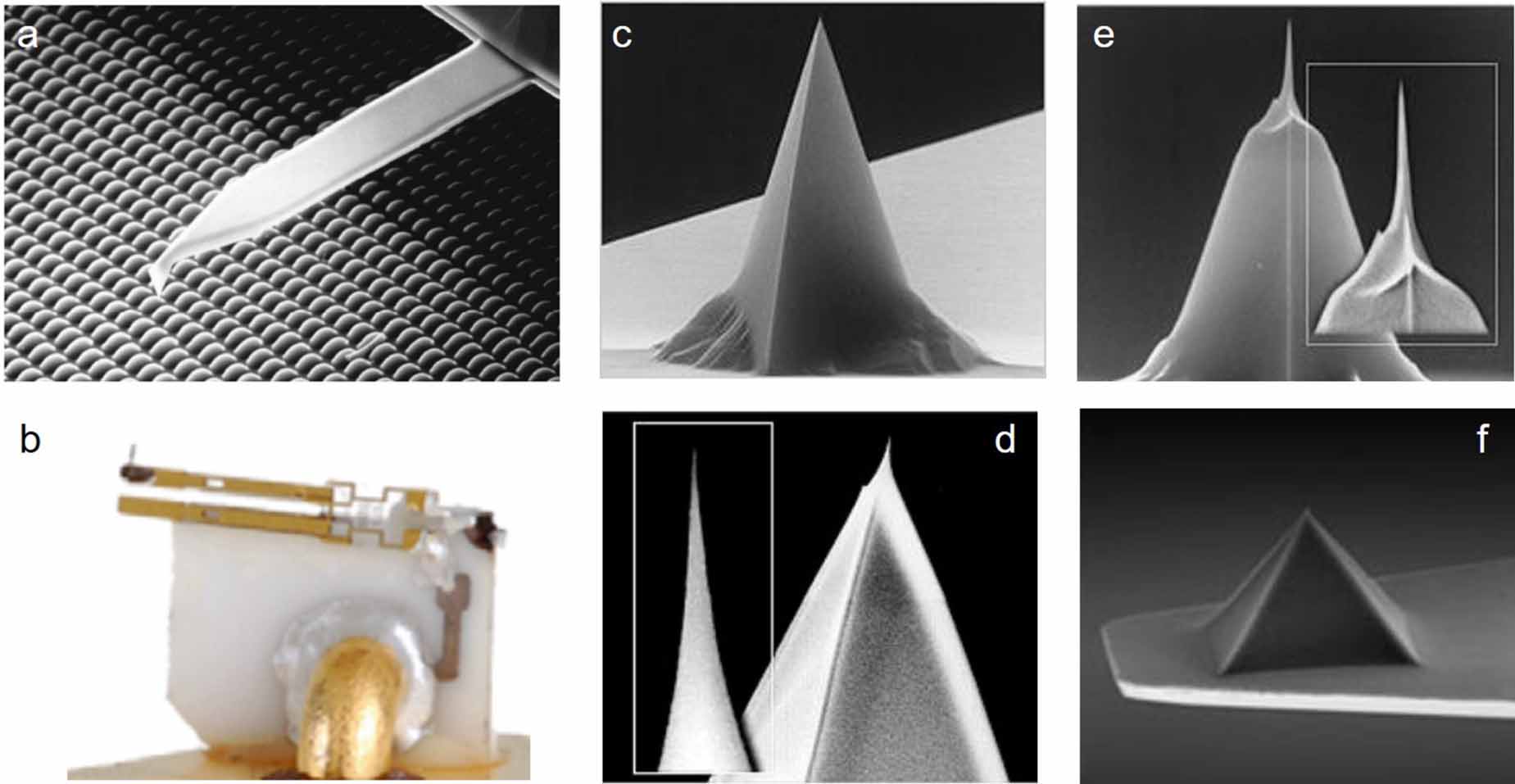
(a) Scanning electron microscopy (SEM) image of a micromachined silicon cantilever with an integrated tip pointing in the [001] crystal direction. (b) Micrograph of a qPlus’sensora cantilever made from a quartz tuning fork [12]. (c)-(f) SEM images of some typical commercial AFM probes: (c) Silicon probe suitable for contact mode. (d) Super sharp silicon probe, suitable for non-contact and tapping modes. (e) High aspect ratio tip. (f) Pyrex-nitride probe. (NanoWorld & PointProbe AFM tip). Reproduced from [12]. © IOP Publishing Ltd. All rights reserved.
Figures of the Article
-
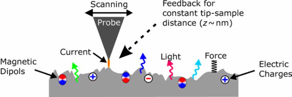
![]() Interactions between the scanning probe microscope probe and the sample surface.
Interactions between the scanning probe microscope probe and the sample surface.
-
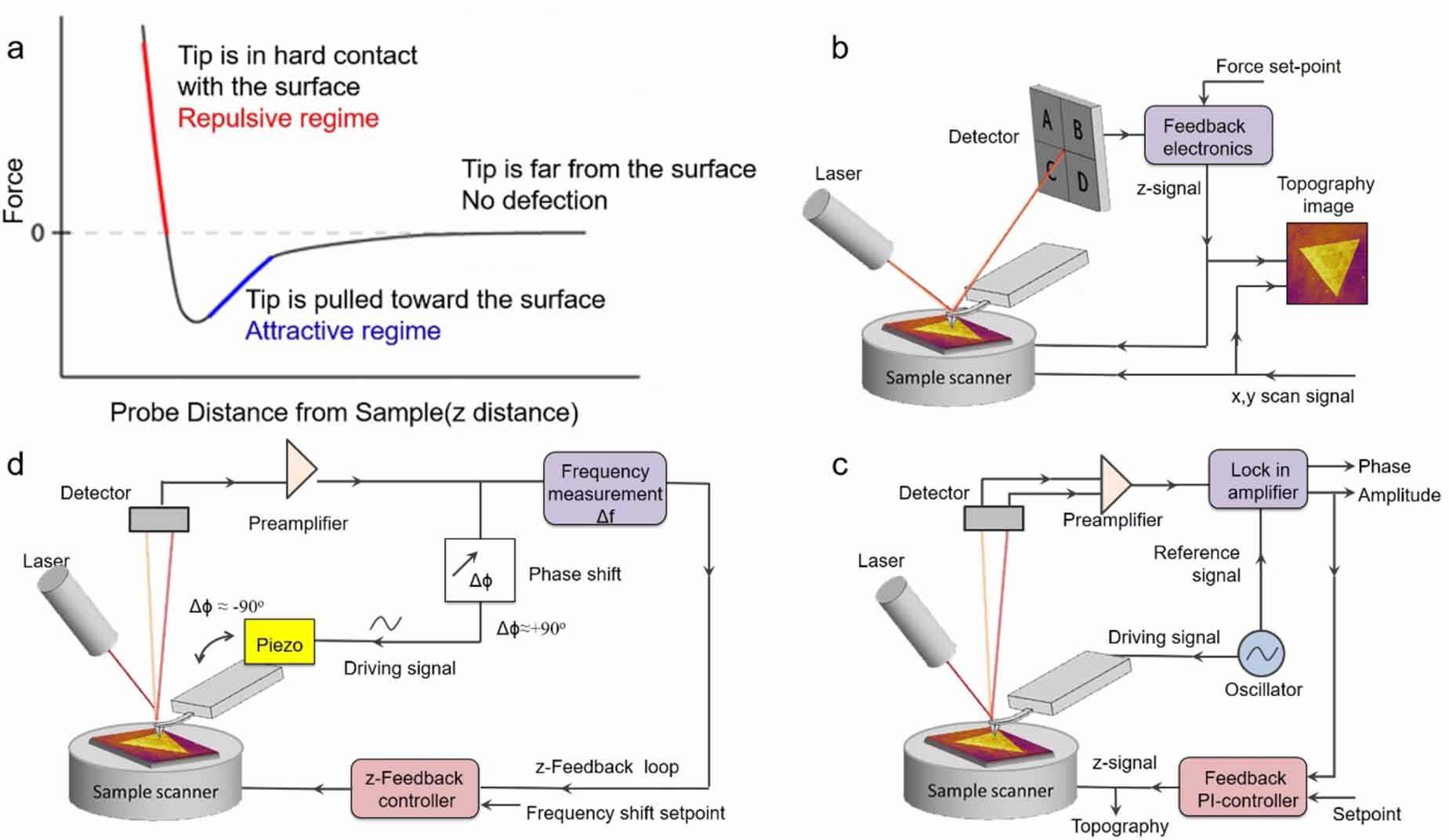
![]() (a) Qualitative behavior of the force between tip and sample as a function of tip-sample distance. (b) and (c) Schematics of atomic force microscopy (AFM) operation: (b) contact mode (static mode), and (c) amplitude modulation mode in dynamic mode. (d) Schematic of frequency modulation detection setup operated in the self-excitation mode. Non-contact AFM.
(a) Qualitative behavior of the force between tip and sample as a function of tip-sample distance. (b) and (c) Schematics of atomic force microscopy (AFM) operation: (b) contact mode (static mode), and (c) amplitude modulation mode in dynamic mode. (d) Schematic of frequency modulation detection setup operated in the self-excitation mode. Non-contact AFM.
-
![]() (a) Scanning electron microscopy (SEM) image of a micromachined silicon cantilever with an integrated tip pointing in the [001] crystal direction. (b) Micrograph of a qPlus’sensora cantilever made from a quartz tuning fork [12]. (c)-(f) SEM images of some typical commercial AFM probes: (c) Silicon probe suitable for contact mode. (d) Super sharp silicon probe, suitable for non-contact and tapping modes. (e) High aspect ratio tip. (f) Pyrex-nitride probe. (NanoWorld & PointProbe AFM tip). Reproduced from [12]. © IOP Publishing Ltd. All rights reserved.
(a) Scanning electron microscopy (SEM) image of a micromachined silicon cantilever with an integrated tip pointing in the [001] crystal direction. (b) Micrograph of a qPlus’sensora cantilever made from a quartz tuning fork [12]. (c)-(f) SEM images of some typical commercial AFM probes: (c) Silicon probe suitable for contact mode. (d) Super sharp silicon probe, suitable for non-contact and tapping modes. (e) High aspect ratio tip. (f) Pyrex-nitride probe. (NanoWorld & PointProbe AFM tip). Reproduced from [12]. © IOP Publishing Ltd. All rights reserved.
-
![]() Resonance frequency range of probes (Asylum Research).
Resonance frequency range of probes (Asylum Research).
-
![]() Sketch map of (a) friction force microscopy (FFM) and (b) transverse shear microscopy (TSM). For FFM (TSM), the scan direction of the AFM tip is perpendicular (parallel) to the long axis of the cantilever. The friction (shear) property of the sample is obtained by detecting the cantilever torsion signal.
Sketch map of (a) friction force microscopy (FFM) and (b) transverse shear microscopy (TSM). For FFM (TSM), the scan direction of the AFM tip is perpendicular (parallel) to the long axis of the cantilever. The friction (shear) property of the sample is obtained by detecting the cantilever torsion signal.
-
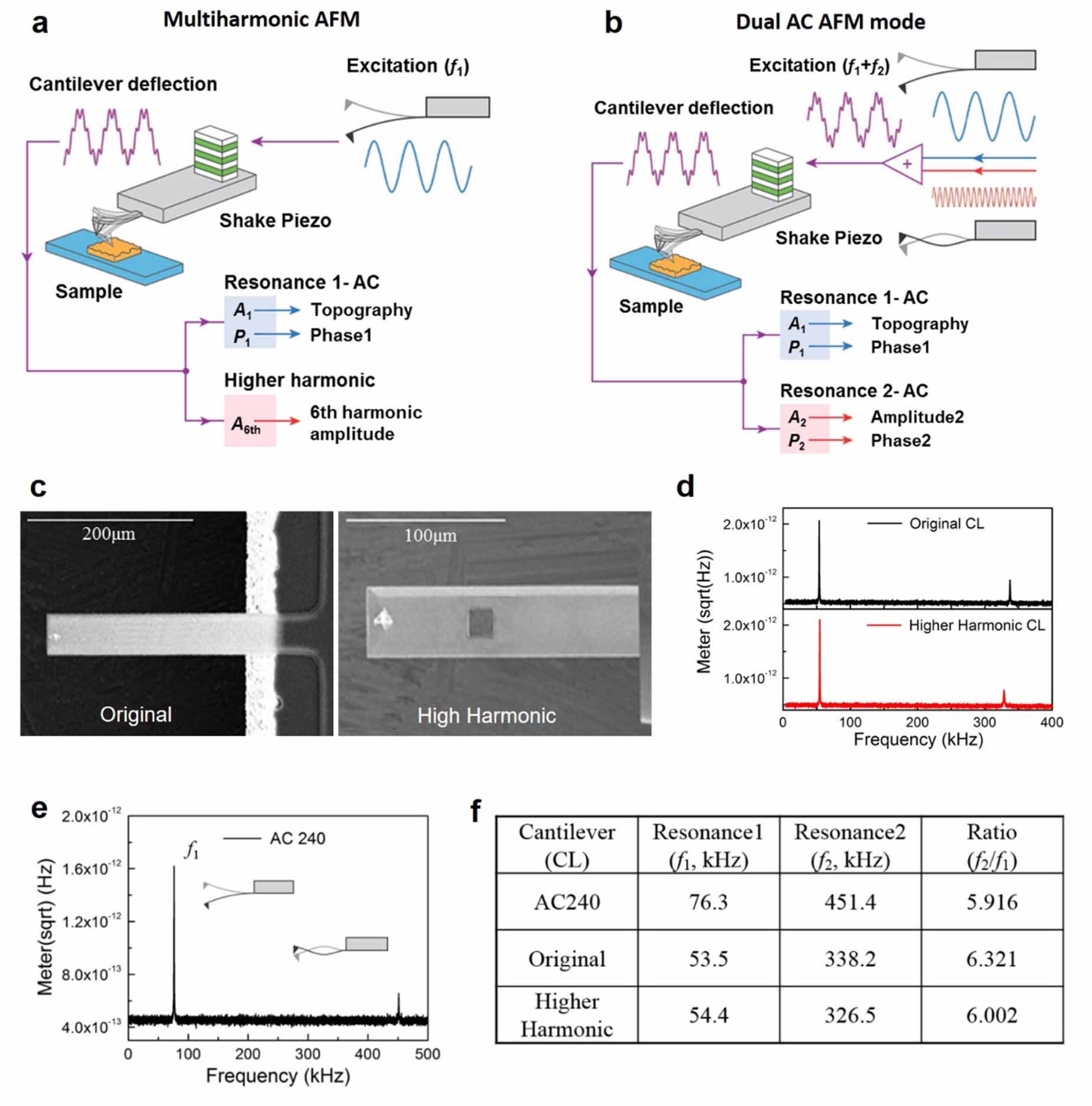
![]() (a) Schematic of the multi-harmonic AFM mode. Recording higher harmonic components introduced by the nonlinearity of tip-sample interaction forces during conventional dynamic AFM imaging while driving the cantilever at its first resonance mode. (b) Schematic of the dual AC AFM mode. The cantilever is simultaneously driven at two eigenmodes (resonant modes), and the amplitude and phase are recorded. (c) SEM images of the original and 6th harmonic probes. (d) Frequency response spectroscopy of the original and 6th harmonic cantilever obtained with the thermal noise spectrum measurement. (e) Frequency response spectroscopy of the AC240 probe obtained with the thermal noise spectrum measurements. (f) Resonance frequencies of the three AFM probes at the first and second resonance mode. Reproduced from [73], with permission from Springer Nature.
(a) Schematic of the multi-harmonic AFM mode. Recording higher harmonic components introduced by the nonlinearity of tip-sample interaction forces during conventional dynamic AFM imaging while driving the cantilever at its first resonance mode. (b) Schematic of the dual AC AFM mode. The cantilever is simultaneously driven at two eigenmodes (resonant modes), and the amplitude and phase are recorded. (c) SEM images of the original and 6th harmonic probes. (d) Frequency response spectroscopy of the original and 6th harmonic cantilever obtained with the thermal noise spectrum measurement. (e) Frequency response spectroscopy of the AC240 probe obtained with the thermal noise spectrum measurements. (f) Resonance frequencies of the three AFM probes at the first and second resonance mode. Reproduced from [73], with permission from Springer Nature.
-
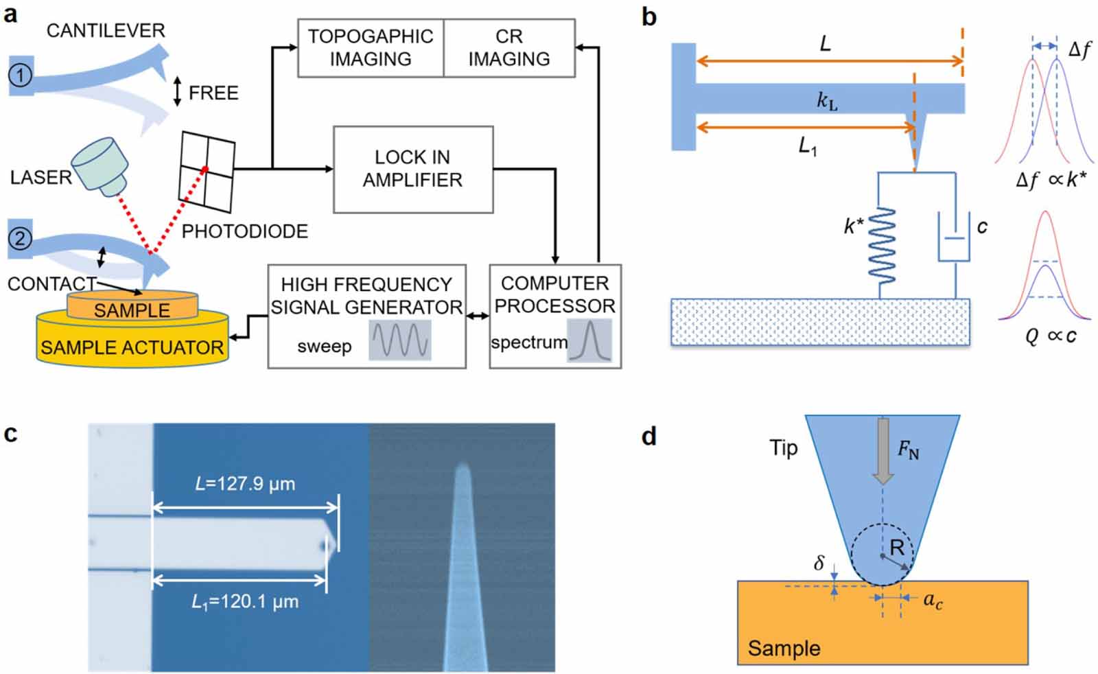
![]() Schematic and mechanical model of contact resonance atomic force microscopy (CR-AFM) and related definitions and characterization of the cantilever used in the experiments for quantitative analysis. (a) Schematic of the CR-AFM experimental setup. (b) Tip-sample contact is modeled as a Kelvin-Voigt mechanical equivalent, where the spring and dashpot represent the contact stiffness (elastic modulus) and viscoelasticity (dissipation), respectively. (c) Close-up view of the tip-sample contact and definitions for quantitative characterization. (d) SEM characterization of the AFM cantilever and tip. Reproduced from [76], with permission from Springer Nature.
Schematic and mechanical model of contact resonance atomic force microscopy (CR-AFM) and related definitions and characterization of the cantilever used in the experiments for quantitative analysis. (a) Schematic of the CR-AFM experimental setup. (b) Tip-sample contact is modeled as a Kelvin-Voigt mechanical equivalent, where the spring and dashpot represent the contact stiffness (elastic modulus) and viscoelasticity (dissipation), respectively. (c) Close-up view of the tip-sample contact and definitions for quantitative characterization. (d) SEM characterization of the AFM cantilever and tip. Reproduced from [76], with permission from Springer Nature.
-
![]() Electronic energy levels between the AFM tip-sample demonstrating the working principle of scanning Kelvin probe microscopy. (a) Tip-sample are separated by a distance d with no electrical contact due to the equal Evac but different EF level. (b) Tip-sample are in electrical contact and electron transfer from the sample with higher EF to the one with lower EF. (c) DC voltage VDC applied between tip-sample readjusts the vacuum level. Reproduced from [91], with permission from Springer Nature.
Electronic energy levels between the AFM tip-sample demonstrating the working principle of scanning Kelvin probe microscopy. (a) Tip-sample are separated by a distance d with no electrical contact due to the equal Evac but different EF level. (b) Tip-sample are in electrical contact and electron transfer from the sample with higher EF to the one with lower EF. (c) DC voltage VDC applied between tip-sample readjusts the vacuum level. Reproduced from [91], with permission from Springer Nature.
-
![]() (a) Schematic of the basic setup for scanning Kelvin probe microscopy (SKPM) technique.
(a) Schematic of the basic setup for scanning Kelvin probe microscopy (SKPM) technique. e is the angular frequency of the applied AC voltage and r is the resonant angular frequency of the cantilever. (b) Drawing map of two scan passes named nap mode. In the first scan, the morphological image is captured using mechanical excitation of the cantilever. The surface potential mapping is acquired in the second scan. The electronic circuit diagram of the first and second scans is given by the black and purple lines. Reproduced from [91], with permission from Springer Nature. -
![]() Schematic of multi-harmonic electrostatic force microscopy (MH-EFM). (a) Schematic of MH-EFM experimental setup. A metal-coated tip was used. Two scan passes are needed in this technique. In the first pass, the resonant frequency amplitude of probe fr is used as feedback to obtain the sample topography. In the second pass (lift mode), an AC bias voltage within the kHz frequency (f) is applied between the tip and sample, and feedback is removed. The amplitude of cantilever vibration at f, f2, and f3 are obtained by Lock-in amplifiers A, A2, and A3, respectively. A is proportional to SP, while A2 is related to the dielectric constant. The amplitude A3 corresponds to the sample carrier concentration. (b) Response of static charges to the charged tip. (c) Response of mobile charges to the charged tip. (d) Relationship between A2, mobile charge carriers, and band gap Egap. Reproduced from [91], with permission from Springer Nature.
Schematic of multi-harmonic electrostatic force microscopy (MH-EFM). (a) Schematic of MH-EFM experimental setup. A metal-coated tip was used. Two scan passes are needed in this technique. In the first pass, the resonant frequency amplitude of probe fr is used as feedback to obtain the sample topography. In the second pass (lift mode), an AC bias voltage within the kHz frequency (f) is applied between the tip and sample, and feedback is removed. The amplitude of cantilever vibration at f, f2, and f3 are obtained by Lock-in amplifiers A, A2, and A3, respectively. A is proportional to SP, while A2 is related to the dielectric constant. The amplitude A3 corresponds to the sample carrier concentration. (b) Response of static charges to the charged tip. (c) Response of mobile charges to the charged tip. (d) Relationship between A2, mobile charge carriers, and band gap Egap. Reproduced from [91], with permission from Springer Nature.
-
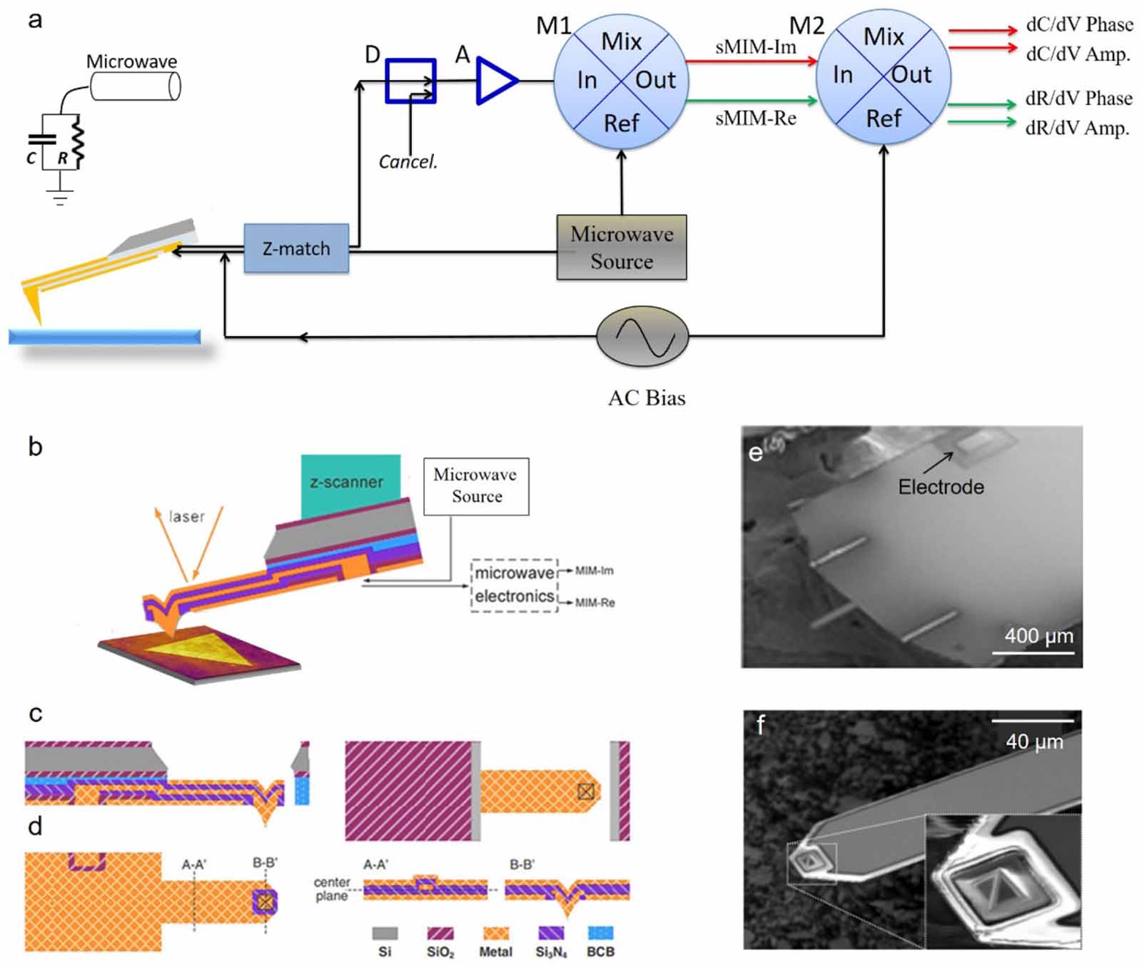
![]() (a) Schematic of sMIM setup. The shielded probe is connected to a microwave source (GHz frequency band). Microwave transmitted into the probe has near-field interactions with the sample, while the reflected microwave is backtracked. The reflected signal is suppressed by the common-mode cancellation through a directional coupler (D), amplified by radio frequency amplifiers (A), and then demodulated by a quadrature mixer (M1). sMIM-Im and sMIM-Re information can be obtained. The signal is further modulated by quadrature mixer M2, and dC/dV and dR/dV are obtained. Inset: schematic of lumped element model. (b) The close-up Schematic of the sMIM probe. (c) The left panels are cross-sectional views and the right panels are top views of the cantilever. (d) Front-view (tip side) of the probe and cross-sectional views of the cantilever (A-A’) and tip apex (B-B’). (e), (f) SEM image of sMIM cantilever and tip. The microwave signal was transmitted to the tip through the electrode, marked in (b), to the tip apex. Reproduced from [115]. © IOP Publishing Ltd. CC BY 3.0.
(a) Schematic of sMIM setup. The shielded probe is connected to a microwave source (GHz frequency band). Microwave transmitted into the probe has near-field interactions with the sample, while the reflected microwave is backtracked. The reflected signal is suppressed by the common-mode cancellation through a directional coupler (D), amplified by radio frequency amplifiers (A), and then demodulated by a quadrature mixer (M1). sMIM-Im and sMIM-Re information can be obtained. The signal is further modulated by quadrature mixer M2, and dC/dV and dR/dV are obtained. Inset: schematic of lumped element model. (b) The close-up Schematic of the sMIM probe. (c) The left panels are cross-sectional views and the right panels are top views of the cantilever. (d) Front-view (tip side) of the probe and cross-sectional views of the cantilever (A-A’) and tip apex (B-B’). (e), (f) SEM image of sMIM cantilever and tip. The microwave signal was transmitted to the tip through the electrode, marked in (b), to the tip apex. Reproduced from [115]. © IOP Publishing Ltd. CC BY 3.0.
-
![]() Setup of an AFM-based scanning thermal microscopy (SThM) system. A thermal control unit delivers the output signal Vout and a balanced Wheatstone bridge maintains the probe mean temperature at a constant value [129]. John Wiley & Sons. [© 2015 WILEY-VCH Verlag GmbH & Co. KGaA, Weinheim].
Setup of an AFM-based scanning thermal microscopy (SThM) system. A thermal control unit delivers the output signal Vout and a balanced Wheatstone bridge maintains the probe mean temperature at a constant value [129]. John Wiley & Sons. [© 2015 WILEY-VCH Verlag GmbH & Co. KGaA, Weinheim].
-
![]() (a) Schematic of the experimental setup for the null-point SThM. (b) SEM images of the SThM probe. Diameter of the thermocouple junction integrated at the apex of the tip is approximately 100 nm, and the tip radius is approximately 50 nm. (c) Principle of quantitative thermal profiling. (d) As the tip approaches the sample, the tip temperature rises gradually due to the heat transfer through the air. When the tip contacts the sample, the tip temperature jumps from Tnc to Tc due to the heat flux through the tip-sample contact. (e) Temperature jumps at different sample temperatures. The slope of the graph, kslope, is 10.9 K K-1 for this particular probe. Reprinted from [141], with the permission of AIP Publishing. Reprinted with permission from [143]. Copyright (2011) American Chemical Society.
(a) Schematic of the experimental setup for the null-point SThM. (b) SEM images of the SThM probe. Diameter of the thermocouple junction integrated at the apex of the tip is approximately 100 nm, and the tip radius is approximately 50 nm. (c) Principle of quantitative thermal profiling. (d) As the tip approaches the sample, the tip temperature rises gradually due to the heat transfer through the air. When the tip contacts the sample, the tip temperature jumps from Tnc to Tc due to the heat flux through the tip-sample contact. (e) Temperature jumps at different sample temperatures. The slope of the graph, kslope, is 10.9 K K-1 for this particular probe. Reprinted from [141], with the permission of AIP Publishing. Reprinted with permission from [143]. Copyright (2011) American Chemical Society.
-
![]() (a) SEM image of a doped silicon probe. (b) Schematic of the principle of thermal probe. (c) Circuit diagram of the local thermal analysis module. (d) Probe electric resistance (Rprobe) vs. temperature (Tprobe = Tprobe-Tair) curve. (e) Demonstration of the thermal tip-sample approach curve. (f) Thermal conductivity (the reciprocal of thermal resistance) vs. tip voltage curve. Thermal conductivity (resistance) is negatively (positively) correlated with the probe voltage. Reproduced from [53] with permission from the Royal Society of Chemistry.
(a) SEM image of a doped silicon probe. (b) Schematic of the principle of thermal probe. (c) Circuit diagram of the local thermal analysis module. (d) Probe electric resistance (Rprobe) vs. temperature (Tprobe = Tprobe-Tair) curve. (e) Demonstration of the thermal tip-sample approach curve. (f) Thermal conductivity (the reciprocal of thermal resistance) vs. tip voltage curve. Thermal conductivity (resistance) is negatively (positively) correlated with the probe voltage. Reproduced from [53] with permission from the Royal Society of Chemistry.
-
![]() Strain-engineered transition metal dichalcogenides (TMDCs) using the thermal expansion coefficient (TEC)-mismatch. (a)-(c) Process schematic through which 2D materials realize strain via the TEC-mismatch between the substrate and TMDC. (a) Tensile strain is achieved when the substrate TEC is less than that of the 2D material, (b) relaxed samples are achieved when the TEC of the substrate and 2D material match, and (c) compressive strain is achieved when the substrate TEC is greater than that of the 2D material. Reprinted with permission from [154]. Copyright (2022) American Chemical Society.
Strain-engineered transition metal dichalcogenides (TMDCs) using the thermal expansion coefficient (TEC)-mismatch. (a)-(c) Process schematic through which 2D materials realize strain via the TEC-mismatch between the substrate and TMDC. (a) Tensile strain is achieved when the substrate TEC is less than that of the 2D material, (b) relaxed samples are achieved when the TEC of the substrate and 2D material match, and (c) compressive strain is achieved when the substrate TEC is greater than that of the 2D material. Reprinted with permission from [154]. Copyright (2022) American Chemical Society.
-
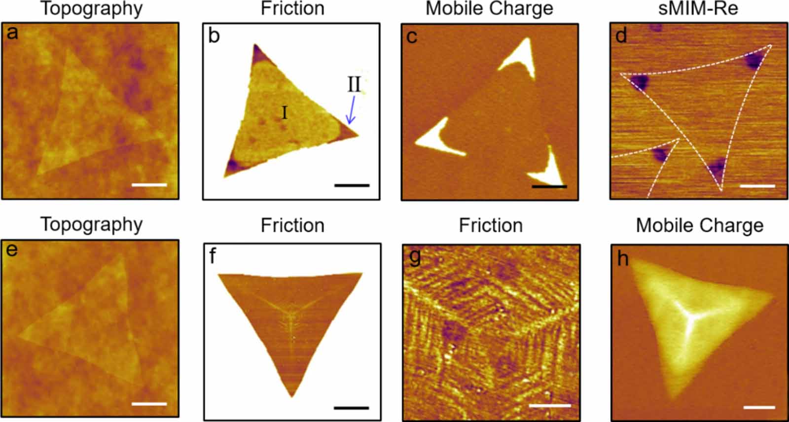
![]() (a) Top (upper panel) and side (lower panel) views of a 2D film at a mesoscopic scale where the edges are identically treated, showing a six-fold symmetry (see cartoon eyes and arrows). (b) Corresponding top and side views at the atomic scale show two completely distinctive edges and a three-fold symmetry. (c), (d) Typical optical and AFM topography of WS2 layer on SiO2/Si substrate. (e) Corresponding local SP images using SKPM. (f) Mobile charge carrier density (MCD) image of WS2 taken in dual harmonic-EFM (DH-EFM). (f) Friction force image of WS2 flakes. Reprinted with permission from [151]. Copyright (2020) American Chemical Society.
(a) Top (upper panel) and side (lower panel) views of a 2D film at a mesoscopic scale where the edges are identically treated, showing a six-fold symmetry (see cartoon eyes and arrows). (b) Corresponding top and side views at the atomic scale show two completely distinctive edges and a three-fold symmetry. (c), (d) Typical optical and AFM topography of WS2 layer on SiO2/Si substrate. (e) Corresponding local SP images using SKPM. (f) Mobile charge carrier density (MCD) image of WS2 taken in dual harmonic-EFM (DH-EFM). (f) Friction force image of WS2 flakes. Reprinted with permission from [151]. Copyright (2020) American Chemical Society.
-
![]() Mechanical properties of hexagonal WS2 flakes. (a) Young’s modulus calculated by Density Function Theory (DFT). (b) AFM topography of the WS2 layer on the SiO2/Si substrate. (c) Close-up AFM topography of the central area of the WS2 layer. (d) Sketch map of contact resonance mode. (e), (f) Elastic modulus and (e) energy dissipation (f) in CR mode. The corresponding topography is shown in (c). (g) Sketch map of FFM. (h), (i) Friction force image of WS2 flakes. The corresponding topography is shown in (b) and (c). Differences in the mechanical property of ZR and KR stem from the C3 atomic arrangement and inherent non-equivalence at the KR and ZR triangle vertexes. Reprinted with permission from [151]. Copyright (2020) American Chemical Society.
Mechanical properties of hexagonal WS2 flakes. (a) Young’s modulus calculated by Density Function Theory (DFT). (b) AFM topography of the WS2 layer on the SiO2/Si substrate. (c) Close-up AFM topography of the central area of the WS2 layer. (d) Sketch map of contact resonance mode. (e), (f) Elastic modulus and (e) energy dissipation (f) in CR mode. The corresponding topography is shown in (c). (g) Sketch map of FFM. (h), (i) Friction force image of WS2 flakes. The corresponding topography is shown in (b) and (c). Differences in the mechanical property of ZR and KR stem from the C3 atomic arrangement and inherent non-equivalence at the KR and ZR triangle vertexes. Reprinted with permission from [151]. Copyright (2020) American Chemical Society.
-
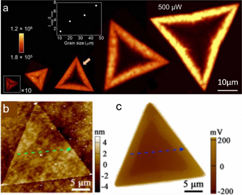
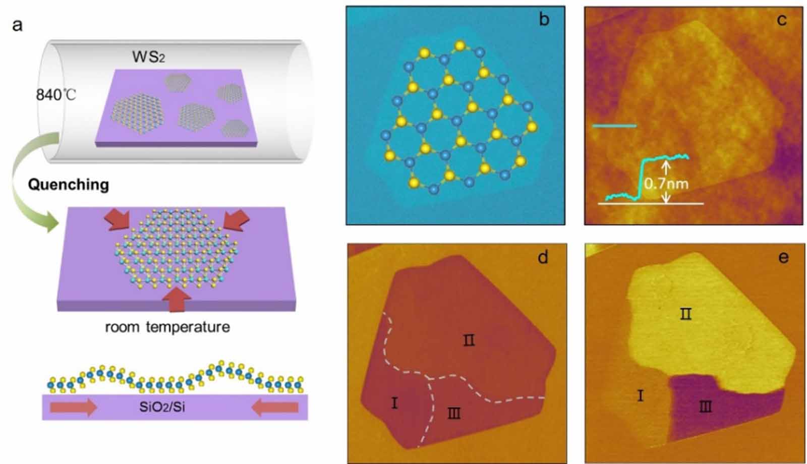
![]() Sample preparation of triangular MoS2 flakes and the introduction of tensile strain. (a) Schematic of traditional low-pressure chemical vapor deposition (CVD) growth process. (b) Introduction of tensile strain applied by the underlying substrate during the fast-cooling process. (c), (e) Size-dependent large-scale optical images of (c) sharp-corner and (e) vein-like MoS2 flakes. (d) Statistical results of the measured sharp-corner and vein-like MoS2 flake size. Optical images of (f) and (g) sharp-corner MoS2 flake and (h) and (i) vein-like MoS2 flake. Scale bars: (c) and (e) 30
Sample preparation of triangular MoS2 flakes and the introduction of tensile strain. (a) Schematic of traditional low-pressure chemical vapor deposition (CVD) growth process. (b) Introduction of tensile strain applied by the underlying substrate during the fast-cooling process. (c), (e) Size-dependent large-scale optical images of (c) sharp-corner and (e) vein-like MoS2 flakes. (d) Statistical results of the measured sharp-corner and vein-like MoS2 flake size. Optical images of (f) and (g) sharp-corner MoS2 flake and (h) and (i) vein-like MoS2 flake. Scale bars: (c) and (e) 30 m; (f)-(i) 5 m. Reproduced from [153]. © IOP Publishing Ltd. All rights reserved. -
![]() (a)-(d) Strain-engineered structures and properties. (a) AFM topography, (b) FFM friction, (c) mobile charge density and (d) sMIM images of sharp-corner MoS2 flake on the SiO2/Si substrate. (e) AFM topography, (f), (g) FFM friction, (h) mobile charge density image of vein-like MoS2 flake on the SiO2/Si substrate. Scale bars: (a)-(c) 6
(a)-(d) Strain-engineered structures and properties. (a) AFM topography, (b) FFM friction, (c) mobile charge density and (d) sMIM images of sharp-corner MoS2 flake on the SiO2/Si substrate. (e) AFM topography, (f), (g) FFM friction, (h) mobile charge density image of vein-like MoS2 flake on the SiO2/Si substrate. Scale bars: (a)-(c) 6 m; (d) 2 m; (e) 5 m; (f) 8 m; (g) 3 m; (f) 5 m. Reproduced from [153]. © IOP Publishing Ltd. All rights reserved. -
![]() (a) Photoluminescence (PL) intensity maps of triangular WS2 monolayers of lateral sizes from 6 to 45
(a) Photoluminescence (PL) intensity maps of triangular WS2 monolayers of lateral sizes from 6 to 45 m. Reprinted with permission from [158]. Copyright (2016) American Chemical Society. (b) AFM image of a typical triangular WS2 flake on SiO2/Si substrate. The sample was prepared by CVD and underwent a fast = cooling process. (c) KPFM SP map of the triangular WS2 flake in panel (b). Reprinted from [162], with the permission of AIP Publishing. -
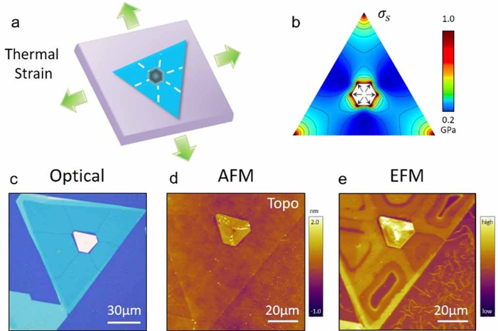
![]() (a) As-grown sample rapidly cooled to room temperature (25 C) from the growth temperature to introduce uniform strain into the sample. (b) von Mises stress of the WS2 flake with the hexagon nucleation center simulated using finite element analysis (FEA). The black lines in (b) are stress isolines, almost perpendicular to the boundary edge. (c), (d) Optical and AFM topography of the six-splitting WS2 layer on the SiO2/Si substrate. (e) MCD image of the WS2 using DH-EFM. Reprinted with permission from [154]. Copyright (2022) American Chemical Society.
(a) As-grown sample rapidly cooled to room temperature (25 C) from the growth temperature to introduce uniform strain into the sample. (b) von Mises stress of the WS2 flake with the hexagon nucleation center simulated using finite element analysis (FEA). The black lines in (b) are stress isolines, almost perpendicular to the boundary edge. (c), (d) Optical and AFM topography of the six-splitting WS2 layer on the SiO2/Si substrate. (e) MCD image of the WS2 using DH-EFM. Reprinted with permission from [154]. Copyright (2022) American Chemical Society.
-
(a) Schematic shape evolution of MoS2 flakes with various S/Mo ratios and growth temperatures. (b)-(h) Optical topographic images of a series of triangular flakes with multi-apex corners. (j), (k) Friction and (l) MCC images of the MoS2 flake with small dual-apex corners. The corresponding optical image is in (d). (m), (n) Frictional and (o) MCC images of the MoS2 flake with larger dual-apex corners. The corresponding optical image is in (e). Reprinted from [17], with the permission of AIP Publishing.
-
![]() Formation mechanism of hierarchal ripple structures. (a)-(d) FFM images of the hierarchical ripple structures in MoS2 with different opening angles. (e)-(h) Evolution of hierarchal ripples in a silk curtain when the confined edges are gradually bent. These ripples are generated through the longitudinal tensile strains applied by the gravity of itself. (i)-(l) Schematic for elucidating the formation and evolution of hierarchical ripples. Reprinted from [17], with the permission of AIP Publishing.
Formation mechanism of hierarchal ripple structures. (a)-(d) FFM images of the hierarchical ripple structures in MoS2 with different opening angles. (e)-(h) Evolution of hierarchal ripples in a silk curtain when the confined edges are gradually bent. These ripples are generated through the longitudinal tensile strains applied by the gravity of itself. (i)-(l) Schematic for elucidating the formation and evolution of hierarchical ripples. Reprinted from [17], with the permission of AIP Publishing.
-
![]() (a) Schematic for TSM and stress distribution originating from stretch deformation. Friction can drive the stretch deformation of a film, and the TSM signals originate from the noncollinearity between the stretch force and deformation direction. If there is strain-induced anisotropic shear deformation, TSM signals will not be zero. (b) Optical image, (c) AFM topography, (d) FFM image, and (e) TSM image of a star-shaped monolayer MoS2 flake sample. In (e), (f), crystallographic labels for AC and ZZ orientations. Every domain of star-shaped monolayer MoS2 is given an identifier from P1 to P7. (g) Shear signal vs. rotation angle curves obtained by randomly selecting P5 domains with the SiO2/Si substrate. (h) Scatterplot diagram of shear signal vs. crystallographic orientation using the AC orientation as the reference direction of 0. All the data points are translated into one period of 60. Reprinted from [18], with the permission of AIP Publishing.
(a) Schematic for TSM and stress distribution originating from stretch deformation. Friction can drive the stretch deformation of a film, and the TSM signals originate from the noncollinearity between the stretch force and deformation direction. If there is strain-induced anisotropic shear deformation, TSM signals will not be zero. (b) Optical image, (c) AFM topography, (d) FFM image, and (e) TSM image of a star-shaped monolayer MoS2 flake sample. In (e), (f), crystallographic labels for AC and ZZ orientations. Every domain of star-shaped monolayer MoS2 is given an identifier from P1 to P7. (g) Shear signal vs. rotation angle curves obtained by randomly selecting P5 domains with the SiO2/Si substrate. (h) Scatterplot diagram of shear signal vs. crystallographic orientation using the AC orientation as the reference direction of 0. All the data points are translated into one period of 60. Reprinted from [18], with the permission of AIP Publishing.
-
![]() (a), (b) Schematic of the puckering effect occurring on the top layer (TL) of MoS2 rather than the bottom layer (BL). (c) Optical, (d) AFM topograp, (e) FFM, and (f) TSM images of bilayer MoS2 on the SiO2/Si substrate. The different MoS2 grains are marked as P11 and P12 for the bottom monolayer and P21 and P22 for the top layer. P0 is the amorphous SiO2/Si substrate. Reproduced from [19], with permission from Springer Nature.
(a), (b) Schematic of the puckering effect occurring on the top layer (TL) of MoS2 rather than the bottom layer (BL). (c) Optical, (d) AFM topograp, (e) FFM, and (f) TSM images of bilayer MoS2 on the SiO2/Si substrate. The different MoS2 grains are marked as P11 and P12 for the bottom monolayer and P21 and P22 for the top layer. P0 is the amorphous SiO2/Si substrate. Reproduced from [19], with permission from Springer Nature.
-
![]() (a) Schematic of CVD growth and cooling process. The in-plane strain is applied onto the WS2 flake via the underlying amorphous SiO2/Si substrate. (b) Optical and (c) AFM topography images of the WS2 flake, scan size: 25
(a) Schematic of CVD growth and cooling process. The in-plane strain is applied onto the WS2 flake via the underlying amorphous SiO2/Si substrate. (b) Optical and (c) AFM topography images of the WS2 flake, scan size: 25 m 25 m. The cyan line shows the height of the WS2 monolayer flake. (d) FM and (e) TSM images of the WS2 flake. The three rippling domains were marked I, II, and III. Reprinted with permission from [156]. Copyright (2021) American Chemical Society. -
![]() Manipulation of ripple orientation on the monolayer WS2 flake. (a)-(c) TSM images of single rippling domain in the monolayer WS2 flake. The insets show the AFM manipulation directions and schematic of the ripple lines in the WS2 flake. In (a), three straight zigzag edges, labeled y (yellow), b (brown), and p (purple), are parallel to the ripple direction in domains I, II, and III, respectively. (d) Schematic illustrating the three rippling domains with the ripple line orientated along the zigzag crystallographic direction of WS2. (e) Schematic of the AFM manipulation directions for the ripple transformation from II and III to I. (f) TSM image of WS2 monolayer flake with single rippling domain. Three sequential TSM images show the AFM manipulation process in the WS2 flake in (f). White arrows illustrate the corresponding writing direction. (g) Snowman’ rippling domain pattern formed by the home-modified AFM lithography. The setpoint (i.e. loading force) of the contact AFM scanning is pixel-dependent according to the pre-defined grayscale image. Reprinted with permission from [156]. Copyright (2021) American Chemical Society.
Manipulation of ripple orientation on the monolayer WS2 flake. (a)-(c) TSM images of single rippling domain in the monolayer WS2 flake. The insets show the AFM manipulation directions and schematic of the ripple lines in the WS2 flake. In (a), three straight zigzag edges, labeled y (yellow), b (brown), and p (purple), are parallel to the ripple direction in domains I, II, and III, respectively. (d) Schematic illustrating the three rippling domains with the ripple line orientated along the zigzag crystallographic direction of WS2. (e) Schematic of the AFM manipulation directions for the ripple transformation from II and III to I. (f) TSM image of WS2 monolayer flake with single rippling domain. Three sequential TSM images show the AFM manipulation process in the WS2 flake in (f). White arrows illustrate the corresponding writing direction. (g) Snowman’ rippling domain pattern formed by the home-modified AFM lithography. The setpoint (i.e. loading force) of the contact AFM scanning is pixel-dependent according to the pre-defined grayscale image. Reprinted with permission from [156]. Copyright (2021) American Chemical Society.
-
![]() Fracture induced by nanoscratch on single-layer MoS2. (a) Schematic of nanoscratch using AFM. The apex radius of 10 nm was chosen, which is not too sharp to pierce the film easily nor too blunt to peel such a huge film. (b) Optical image of MoS2 film after scratch. (c) FFM image of the scratched domain with distinctive crack morphology. Normal load increases from 50 to 70
Fracture induced by nanoscratch on single-layer MoS2. (a) Schematic of nanoscratch using AFM. The apex radius of 10 nm was chosen, which is not too sharp to pierce the film easily nor too blunt to peel such a huge film. (b) Optical image of MoS2 film after scratch. (c) FFM image of the scratched domain with distinctive crack morphology. Normal load increases from 50 to 70 N. (d), (e) Close-up of the domain in white dashed frame in (c). In (d), periodical zigzag cracks along the scratch path. In (e), the forepart of the whole fracture. (f) FFM image of a string of cracks along the armchair direction. The scratch is from left to right, as shown by the arrow. The head shape of the crack is flat. (g) String of cracks along the zigzag direction, from up to down. The head shape of the crack is angular. Reproduced from [177]. © IOP Publishing Ltd. All rights reserved. In (c)-(e), scale bars here are 1.0 m. In (f), (g), scale bars here are 0.5 m. -
![]() (a) Schematic of the friction process and KPFM measurement system. KPFM image of graphene (b) before and (c) after rubbing. (d) Potential difference generated by tunneling triboelectrification, VTT, along the blue dashed line in (c) after 0 and 72 h; VTT is well preserved even after 72 h. (e) VTT as a function of time. The best fit (blue line) is the sum of two decaying exponential terms, each with its own time constant. Reproduced from [182]. CC BY 4.0.
(a) Schematic of the friction process and KPFM measurement system. KPFM image of graphene (b) before and (c) after rubbing. (d) Potential difference generated by tunneling triboelectrification, VTT, along the blue dashed line in (c) after 0 and 72 h; VTT is well preserved even after 72 h. (e) VTT as a function of time. The best fit (blue line) is the sum of two decaying exponential terms, each with its own time constant. Reproduced from [182]. CC BY 4.0.
-
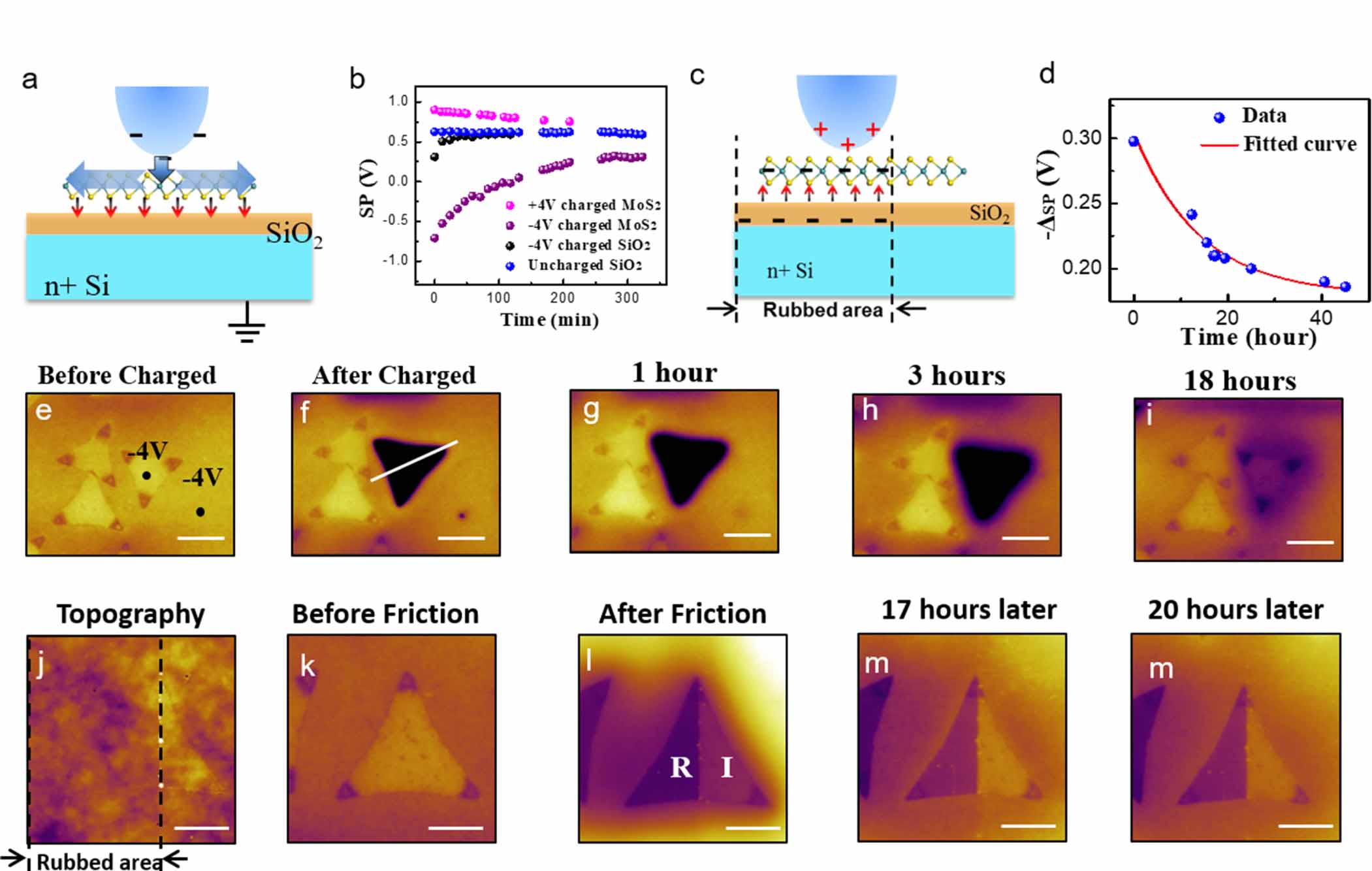
![]() (a) Schematic of charge transfer with tip and MoS2/SiO2 contacting. (b) Profiles of SP vs. time. (c) Schematic of charge transfer between the tip and MoS2/SiO2 with tip friction on MoS2/SiO2. (d) Profiles of SP vs. time. (e) MoS2 SP before charging. Contact voltages applied by the AFM tip are marked. (f)-(i) Series of SP images taken in the same region after biased tip contacting MoS2. (e)-(i) Scale bars are 5
(a) Schematic of charge transfer with tip and MoS2/SiO2 contacting. (b) Profiles of SP vs. time. (c) Schematic of charge transfer between the tip and MoS2/SiO2 with tip friction on MoS2/SiO2. (d) Profiles of SP vs. time. (e) MoS2 SP before charging. Contact voltages applied by the AFM tip are marked. (f)-(i) Series of SP images taken in the same region after biased tip contacting MoS2. (e)-(i) Scale bars are 5 m. (j) AFM topography of MoS2 on SiO2/Si substrates after rubbing. Rubbed area is marked. (k) SP images of the neutral sample. (l)-(n) AFM images of MoS2 layer after triboelectrification, showing a sharp edge between rubbed (marked R) and intact (marked I) MoS2. (j)-(m) Scale bars are 4 m. Reproduced from [30]. © IOP Publishing Ltd. All rights reserved. -
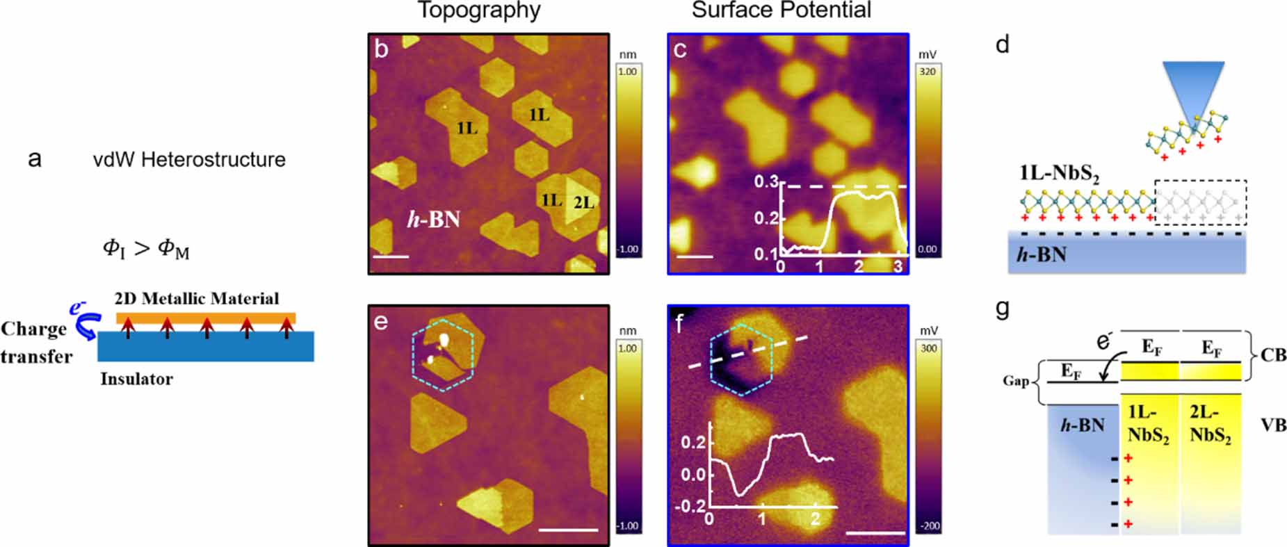
![]() (a) Charge transfer between the 2D metal layer and insulator. (b), (c) AFM topography and SP of NbS2/BN using SKPM. Inset: SP profiles along dash lines in (c). (d) Schematic of post-exposed h-BN surface preparation. Post-exposed h-BN surface is the h-BN surface covered by NbS2 in the growth process but exposed after peeling the NbS2 using AFM tips. NbS2 layers framed by the dashed box stand for the stripped part before peeling. Charge distribution at the 1L-NbS2/BN interface and post-exposed h-BN surface is also shown. (e) AFM topography after partly peeling NbS2, the dash hexagon shows the position of the NbS2 layer before peeling. (f) SP image of the post-exposed h-BN surface. Inset: SP profiles along the dash lines in (f). (g) Schematic energy band diagram of NbS2/BN showing electron transfer from 1L-NbS2 to h-BN. Scale bars are 1
(a) Charge transfer between the 2D metal layer and insulator. (b), (c) AFM topography and SP of NbS2/BN using SKPM. Inset: SP profiles along dash lines in (c). (d) Schematic of post-exposed h-BN surface preparation. Post-exposed h-BN surface is the h-BN surface covered by NbS2 in the growth process but exposed after peeling the NbS2 using AFM tips. NbS2 layers framed by the dashed box stand for the stripped part before peeling. Charge distribution at the 1L-NbS2/BN interface and post-exposed h-BN surface is also shown. (e) AFM topography after partly peeling NbS2, the dash hexagon shows the position of the NbS2 layer before peeling. (f) SP image of the post-exposed h-BN surface. Inset: SP profiles along the dash lines in (f). (g) Schematic energy band diagram of NbS2/BN showing electron transfer from 1L-NbS2 to h-BN. Scale bars are 1 m. Reproduced from [92]. © IOP Publishing Ltd. All rights reserved. -
![]() (a) AFM and (b) KPFM images of the MoS2/PbI2 heterostructures. (c) Schematic of band energy of MoS2/PbI2 heterostructures. Reproduced from [185], with permission from Springer Nature.
(a) AFM and (b) KPFM images of the MoS2/PbI2 heterostructures. (c) Schematic of band energy of MoS2/PbI2 heterostructures. Reproduced from [185], with permission from Springer Nature.
-
![]() (a), (b) Topography and friction images (11
(a), (b) Topography and friction images (11 m 24 m) of water-intercalated graphene on mica after mechanical cleavage in air. (c), (d) Magnified topography and friction images (7 m 7 m) from the blue box in (b), where the labels represent a bare mica, b SLG, c SLG + 1 W, d BLG + 1 W, e BLG, f SLG, and g bare mica. (e), (f) Section line of the height and friction along the red lines in (c) and (d). (g) Schematic showing the variable friction behavior using an AFM tip, depending on the sublayer composition. Labels (a)-(g) in the tips match areas (a)-(g) in (c). Reproduced from [190], with permission from Springer Nature. -
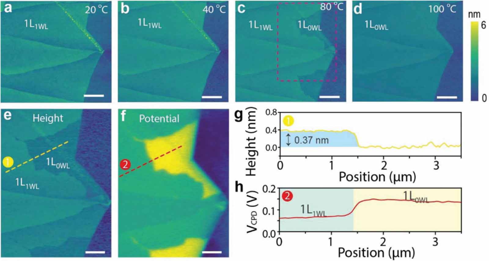
![]() (a)-(d) Recorded in-situ AFM height images of graphene supported on SiO2/Si substrate from room temperature (25 C) to 100 C. The scale bars are 2
(a)-(d) Recorded in-situ AFM height images of graphene supported on SiO2/Si substrate from room temperature (25 C) to 100 C. The scale bars are 2 m. (e) Magnified AFM height image and (f) corresponding SP recorded by SKPM at 80 C. The scale bars are 1 m. (g) Height and (h) VCPD line profiles measured along the yellow and red dashed lines marked in (e) and (f), respectively. Reproduced from [191] with permission from the Royal Society of Chemistry. -
![]() (a) Optical microscopic image of the mechanically exfoliating folding few-layers graphene flake on SiO2/Si substrate. It can encapsulate water molecules because of its mechanical strength and chemical stability. (b) Basic principle of MF-AFM. The MF-AFM amplitude (AMF) reflects the local mechanical properties (e.g. elastic modulus and viscoelasticity) of the sample and has subsurface detection capability. MF-AFM observes the different phase structures of intercalated water layers. (c), (d) Topography and A6th image of water intercalated sample in multi-harmonic mode. Scan size: 30
(a) Optical microscopic image of the mechanically exfoliating folding few-layers graphene flake on SiO2/Si substrate. It can encapsulate water molecules because of its mechanical strength and chemical stability. (b) Basic principle of MF-AFM. The MF-AFM amplitude (AMF) reflects the local mechanical properties (e.g. elastic modulus and viscoelasticity) of the sample and has subsurface detection capability. MF-AFM observes the different phase structures of intercalated water layers. (c), (d) Topography and A6th image of water intercalated sample in multi-harmonic mode. Scan size: 30 m. (e) Histogram distribution of A6th/elastic modulus extracted from (d). Arbitrarily units (a.u.) qualitatively describe A6th/elastic modulus of the interfacial water layer. (f), (g) Topography and A2 image of the water intercalated sample in dual AC mode. Scan size: 15 m. (h) Histogram distribution of A2/dissipation extracted from (g). Reproduced from [73], with permission from Springer Nature. -
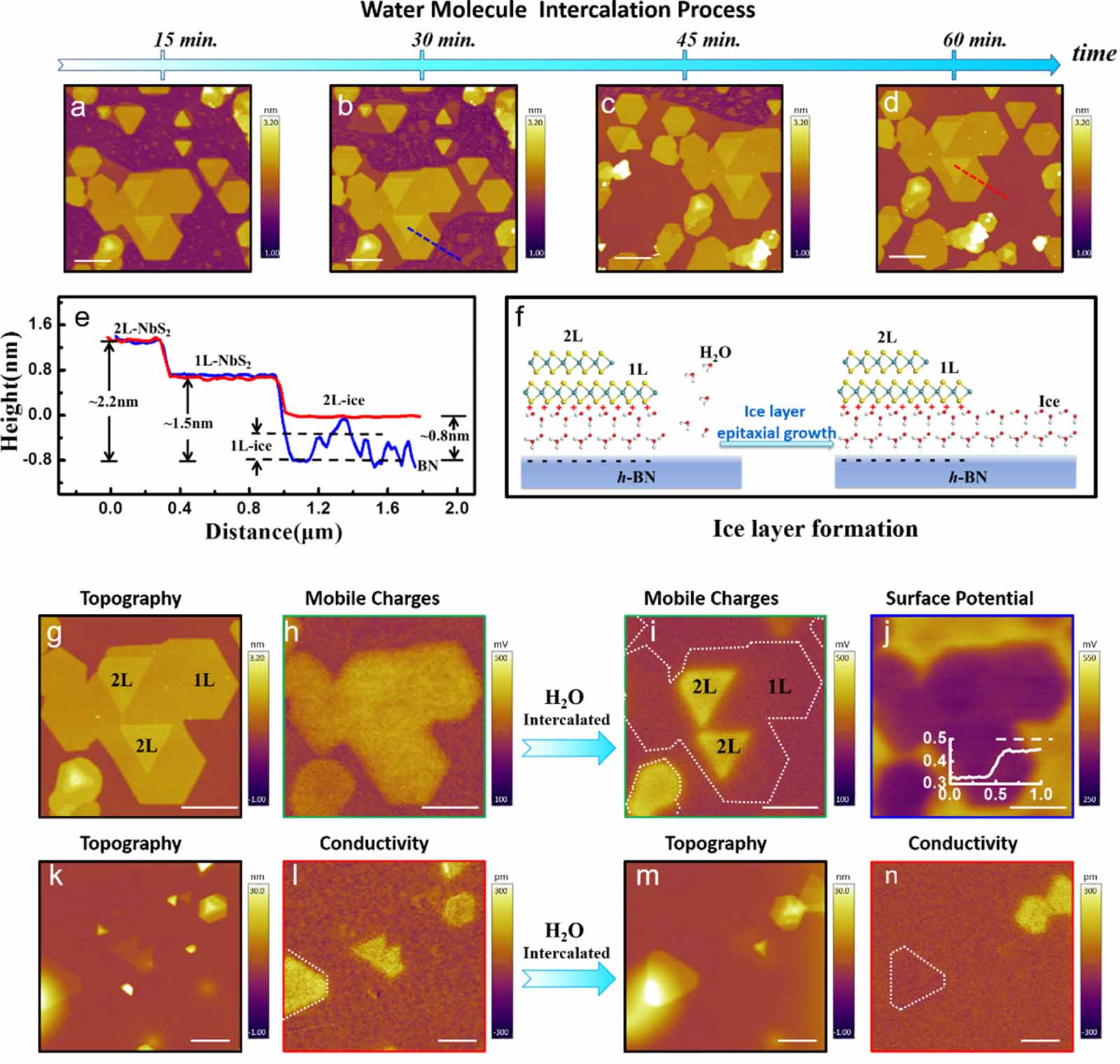
![]() (a)-(d) Water molecules intercalate at the interface and grow on the sample surface. (e) Section lines during (blue line) and after (red line) water intercalation. (f) Schematic of evolution process and structure diagram of water molecule intercalation at the 1L-NbS2/BN heterointerface. (g), (h) AFM topography and MCC images of pristine NbS2/BN heterostructures. (i), (j) MCC and SP images of water-intercalated heterostructures. (k)-(n) Topography and conductivity images of (k), (l) pristine and (m), (n) water-intercalated NbS2/BN heterostructures using sMIM mode. Scale bars are 1
(a)-(d) Water molecules intercalate at the interface and grow on the sample surface. (e) Section lines during (blue line) and after (red line) water intercalation. (f) Schematic of evolution process and structure diagram of water molecule intercalation at the 1L-NbS2/BN heterointerface. (g), (h) AFM topography and MCC images of pristine NbS2/BN heterostructures. (i), (j) MCC and SP images of water-intercalated heterostructures. (k)-(n) Topography and conductivity images of (k), (l) pristine and (m), (n) water-intercalated NbS2/BN heterostructures using sMIM mode. Scale bars are 1 m. Reproduced from [92]. © IOP Publishing Ltd. All rights reserved. -
![]() (a) Heater-sample thermal contact resistance (RX) image acquired at TS = 220 K for different areas of interest. (b) Schematic of the heat transport from the tip to the substrate through 2D structures. [200] John Wiley & Sons. [© 2019 WILEY-VCH Verlag GmbH & Co. KGaA, Weinheim]. (c) Optical and AFM images of a MoS2-WS2 heterostructure. (d) Raman map of the MoS2-WS2 heterostructure device. (e), (f) Temperature rise profiles in this device at different dissipated electrical power at VG = +60 V. The heating predominantly occurs on the WS2-metal vertical junction, and the lateral interface does not contribute to heat localization. The green arrows in (f) show the hot-spot position. [201] John Wiley & Sons. [© 2019 WILEY-VCH Verlag GmbH & Co. KGaA, Weinheim].
(a) Heater-sample thermal contact resistance (RX) image acquired at TS = 220 K for different areas of interest. (b) Schematic of the heat transport from the tip to the substrate through 2D structures. [200] John Wiley & Sons. [© 2019 WILEY-VCH Verlag GmbH & Co. KGaA, Weinheim]. (c) Optical and AFM images of a MoS2-WS2 heterostructure. (d) Raman map of the MoS2-WS2 heterostructure device. (e), (f) Temperature rise profiles in this device at different dissipated electrical power at VG = +60 V. The heating predominantly occurs on the WS2-metal vertical junction, and the lateral interface does not contribute to heat localization. The green arrows in (f) show the hot-spot position. [201] John Wiley & Sons. [© 2019 WILEY-VCH Verlag GmbH & Co. KGaA, Weinheim].
-
![]() (a) Series of friction images of the MoS2 with increasing normal force. (b) The curves of the friction signals of the sample and substrate vs. normal forces. Data are extracted from (a). Inset is the enlarged view of the dashed rectangle. The 0L, 1L, and 2L represent the substrate, monolayer film, and bilayer film, respectively. (c) Series of in-situ TR images of the MoS2 with increasing normal force, corresponding to (a). (d) Relative dynamic/static thermal resistances vs. normal forces. Data are extracted from (c). Resistance values are the difference values of the sample and substrate. (e) Schematic illustration of static and dynamic TR principle. (f) Thermal resistance image of WS2. The crystallographic orientations of armchair (AC) and zigzag (ZZ) based on the primitive growth edges of WS2 are marked. (g) Polar diagram of the relative dynamic thermal resistance vs. crystallographic orientation of 1L-WS2. The relative dynamic TR values are extracted from SThM images by changing the scan angles. Reproduced from [53] with permission from the Royal Society of Chemistry.
(a) Series of friction images of the MoS2 with increasing normal force. (b) The curves of the friction signals of the sample and substrate vs. normal forces. Data are extracted from (a). Inset is the enlarged view of the dashed rectangle. The 0L, 1L, and 2L represent the substrate, monolayer film, and bilayer film, respectively. (c) Series of in-situ TR images of the MoS2 with increasing normal force, corresponding to (a). (d) Relative dynamic/static thermal resistances vs. normal forces. Data are extracted from (c). Resistance values are the difference values of the sample and substrate. (e) Schematic illustration of static and dynamic TR principle. (f) Thermal resistance image of WS2. The crystallographic orientations of armchair (AC) and zigzag (ZZ) based on the primitive growth edges of WS2 are marked. (g) Polar diagram of the relative dynamic thermal resistance vs. crystallographic orientation of 1L-WS2. The relative dynamic TR values are extracted from SThM images by changing the scan angles. Reproduced from [53] with permission from the Royal Society of Chemistry.


Related articles
-
2025, 4(3) DOI: 10.1088/2752-5724/ade60f
-
2025, 4(3) DOI: 10.1088/2752-5724/ade4e3
-
2025, 4(1) DOI: 10.1088/2752-5724/ada8c5
-
2025, 4(1) DOI: 10.1088/2752-5724/ad93ea
-
2025, 4(1) DOI: 10.1088/2752-5724/ada172
-
2023, 2(2) DOI: 10.1088/2752-5724/acc3b3
-
2023, 2(1) DOI: 10.1088/2752-5724/acba36
-
2022, 1(3) DOI: 10.1088/2752-5724/ac84f5
-
2022, 1(1) DOI: 10.1088/2752-5724/ac49e3


